


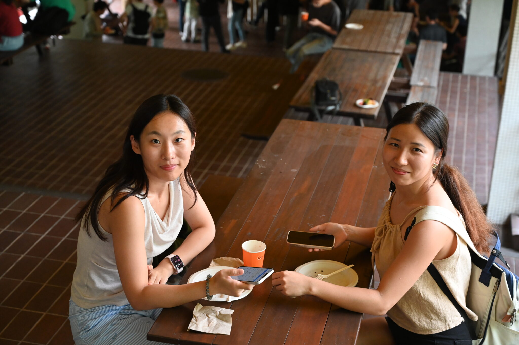
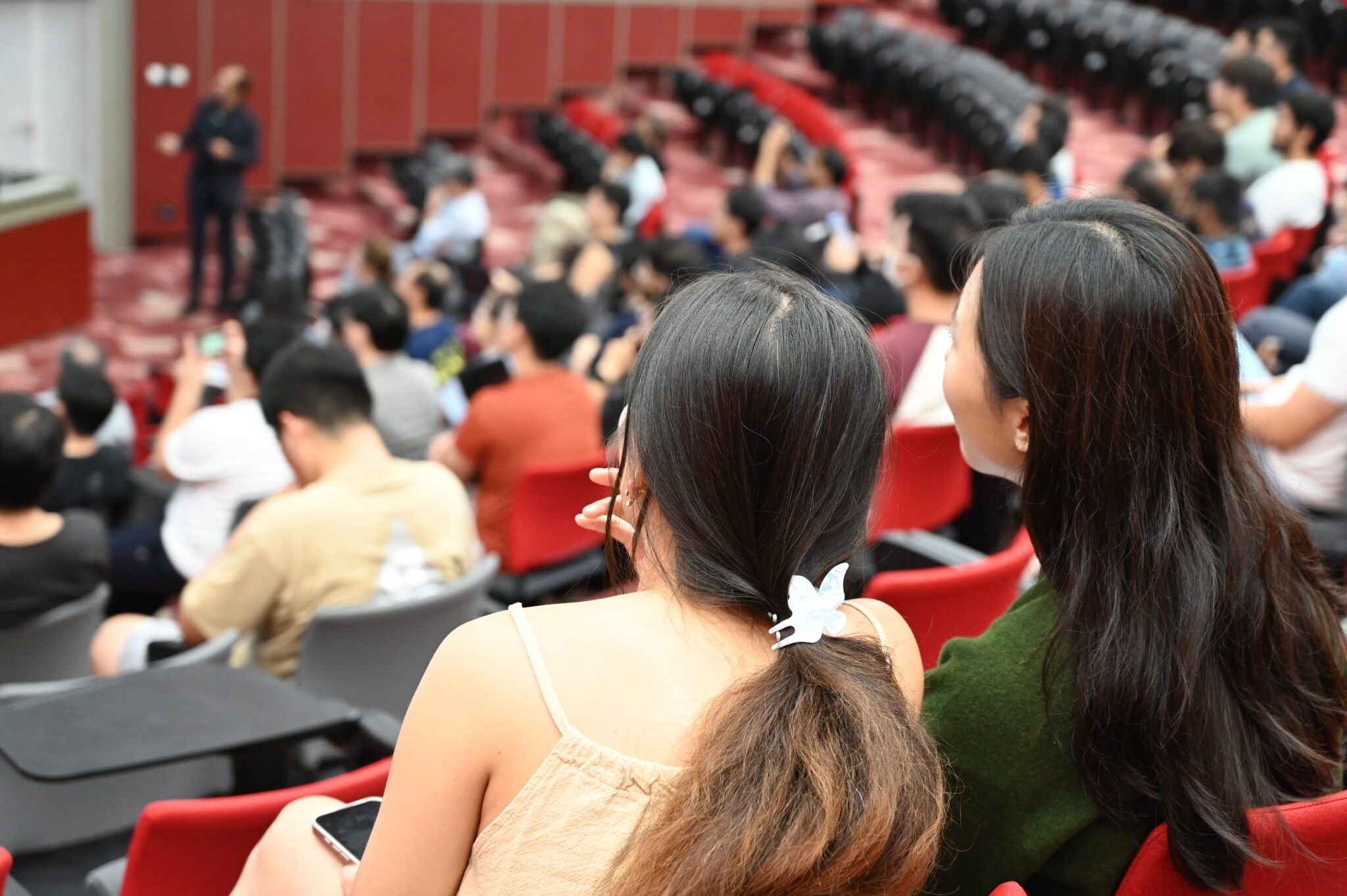
Our events and seminars feature a diverse range of speakers who share their research findings as well as showcase applications across diverse domains such as nanotechnology, renewable energy, healthcare, electronics, and other real-world applications at the forefront of innovation in advanced materials.
Come discover the latest here where we invite speakers to share their research findings, and where applications in materials science and engineering come to life.
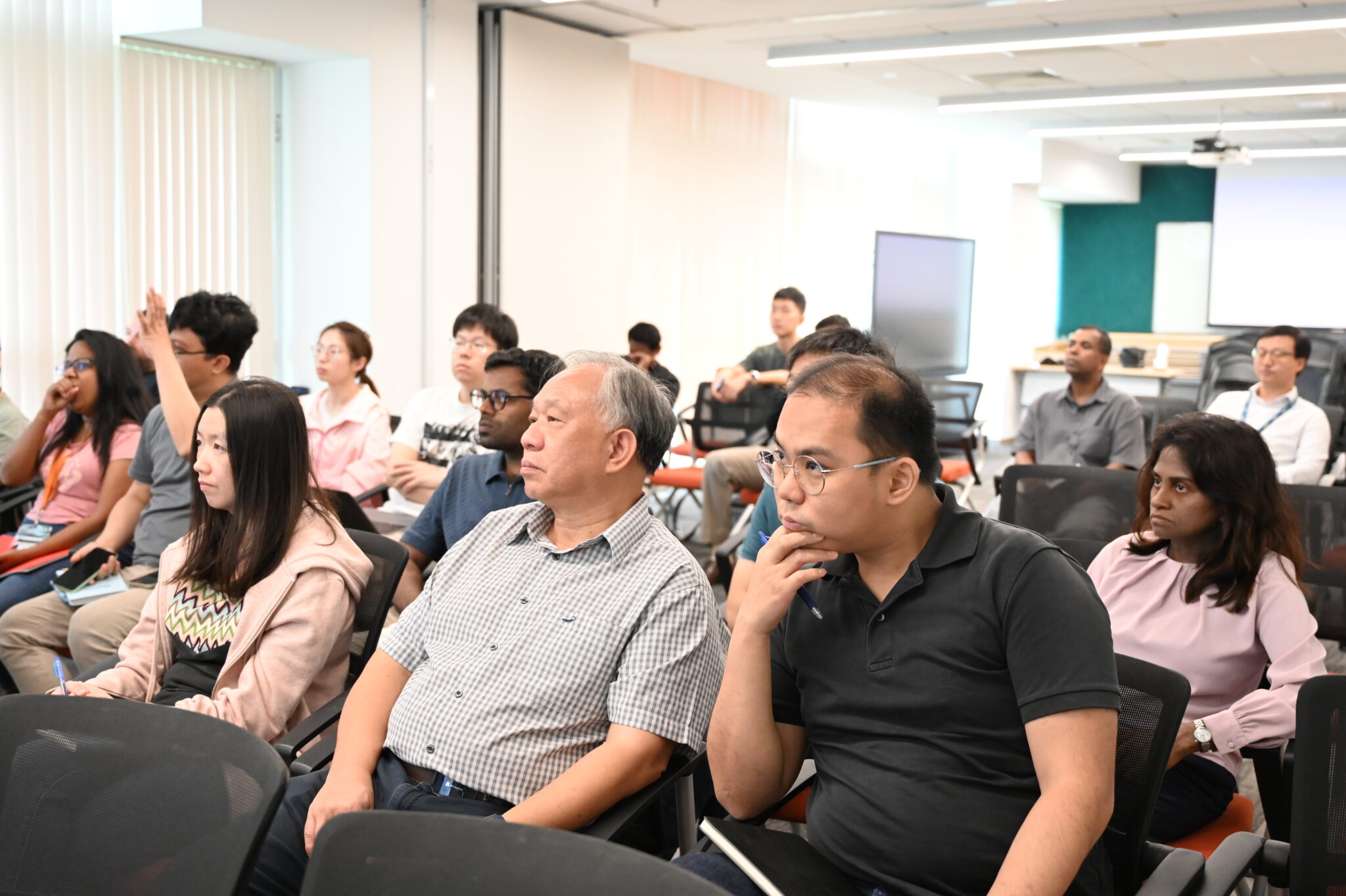
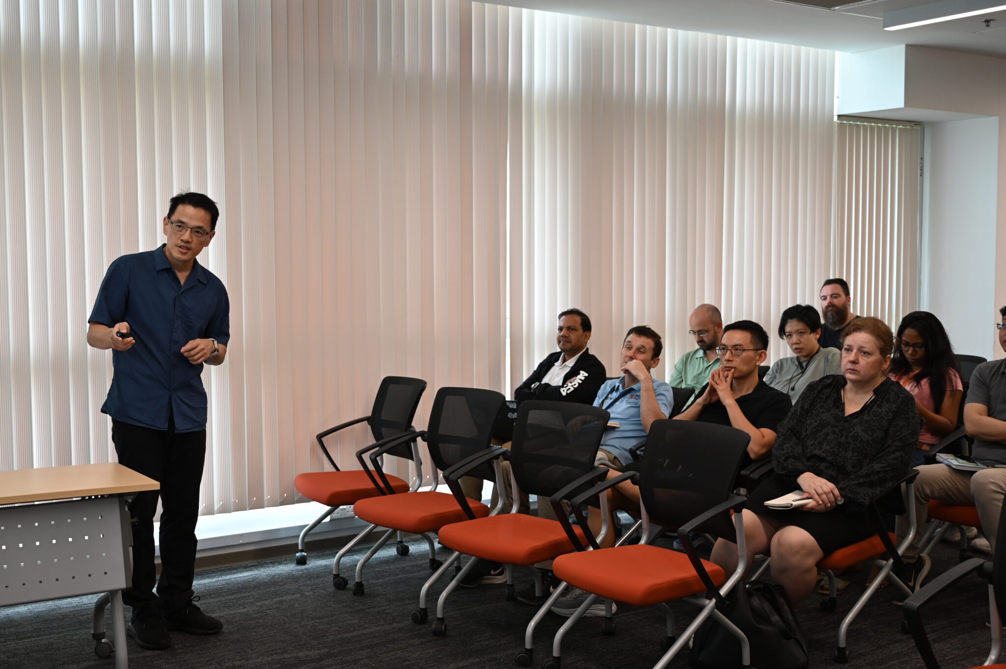
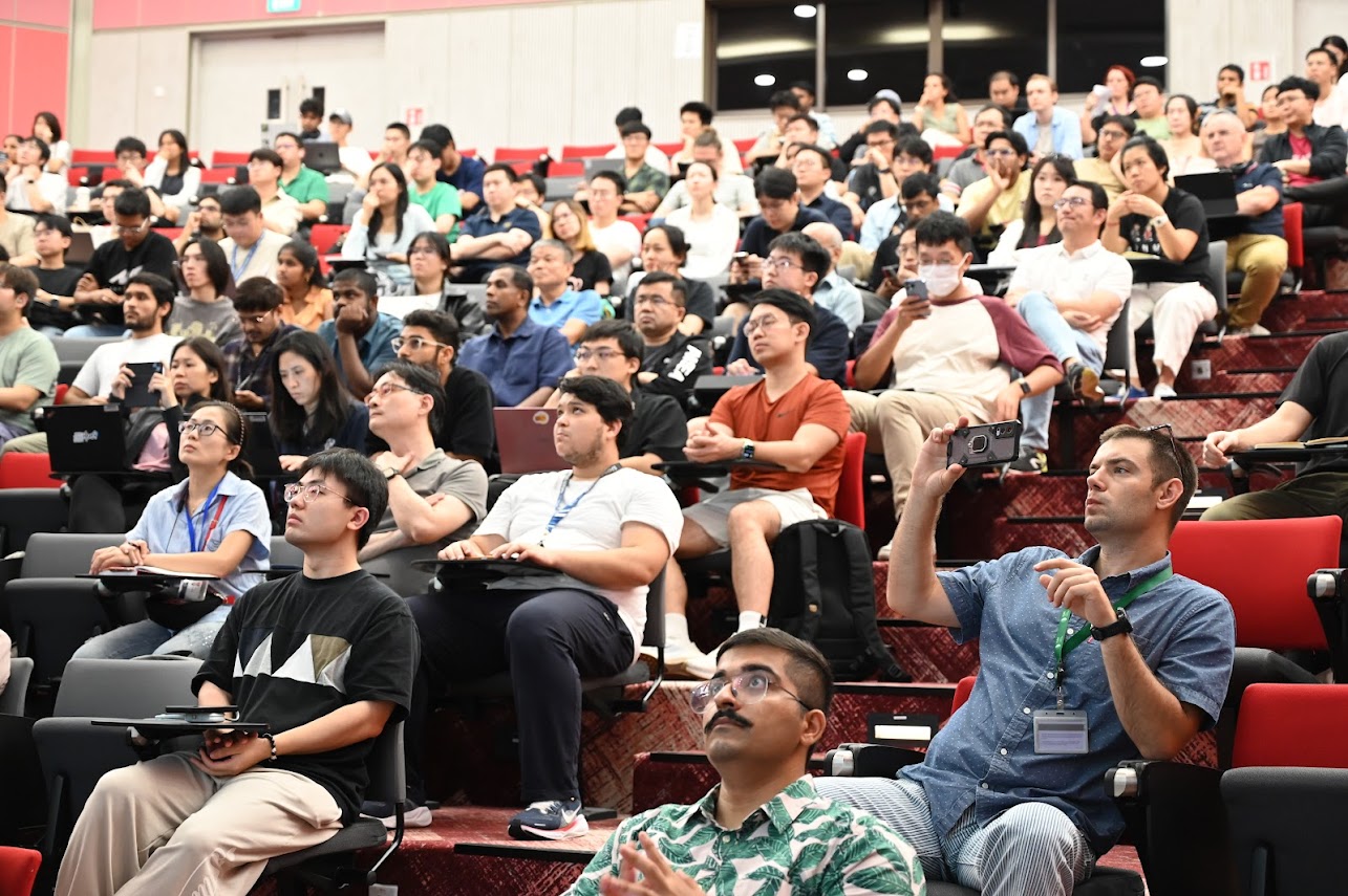
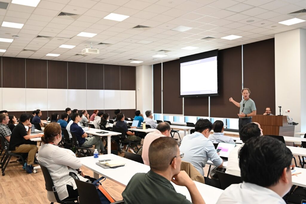
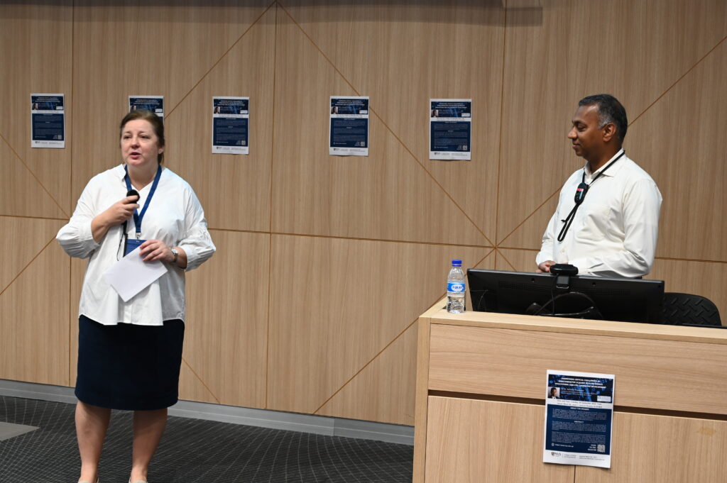
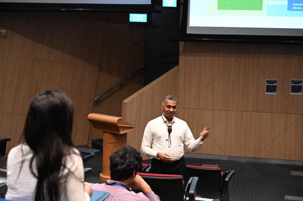
Date & Time: Wednesday, 11th February 2026, 11am to 12pm
Venue: Eureka Conference Room 1 & 2 (E6-06), NUS.
College of Design and Engineering (CDE), 9 Engineering Drive 1, NUS
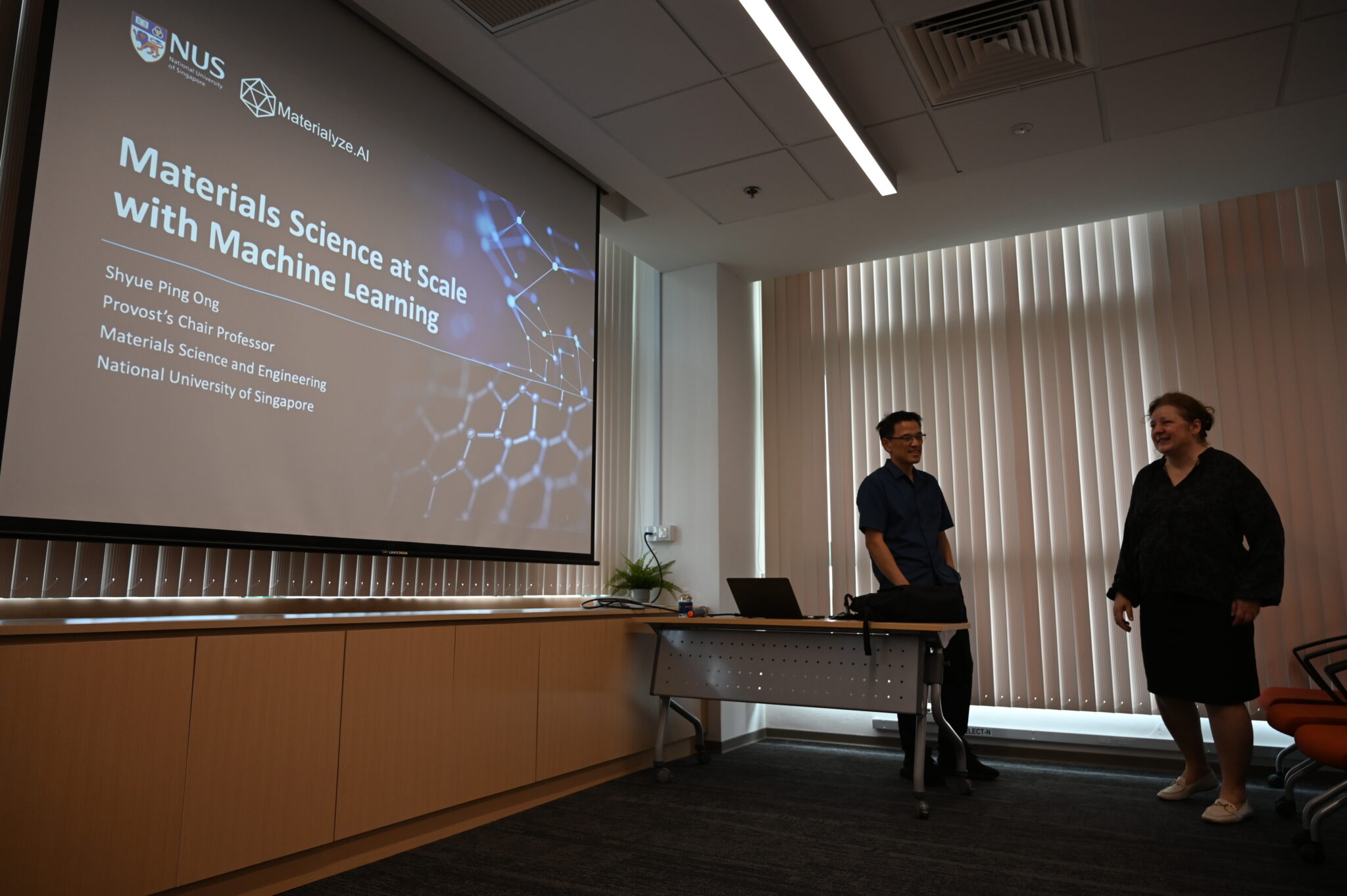
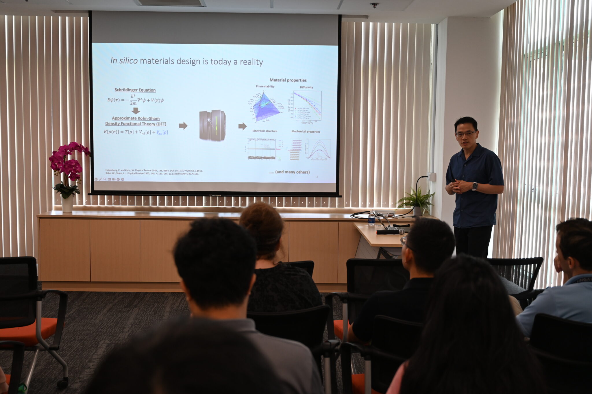
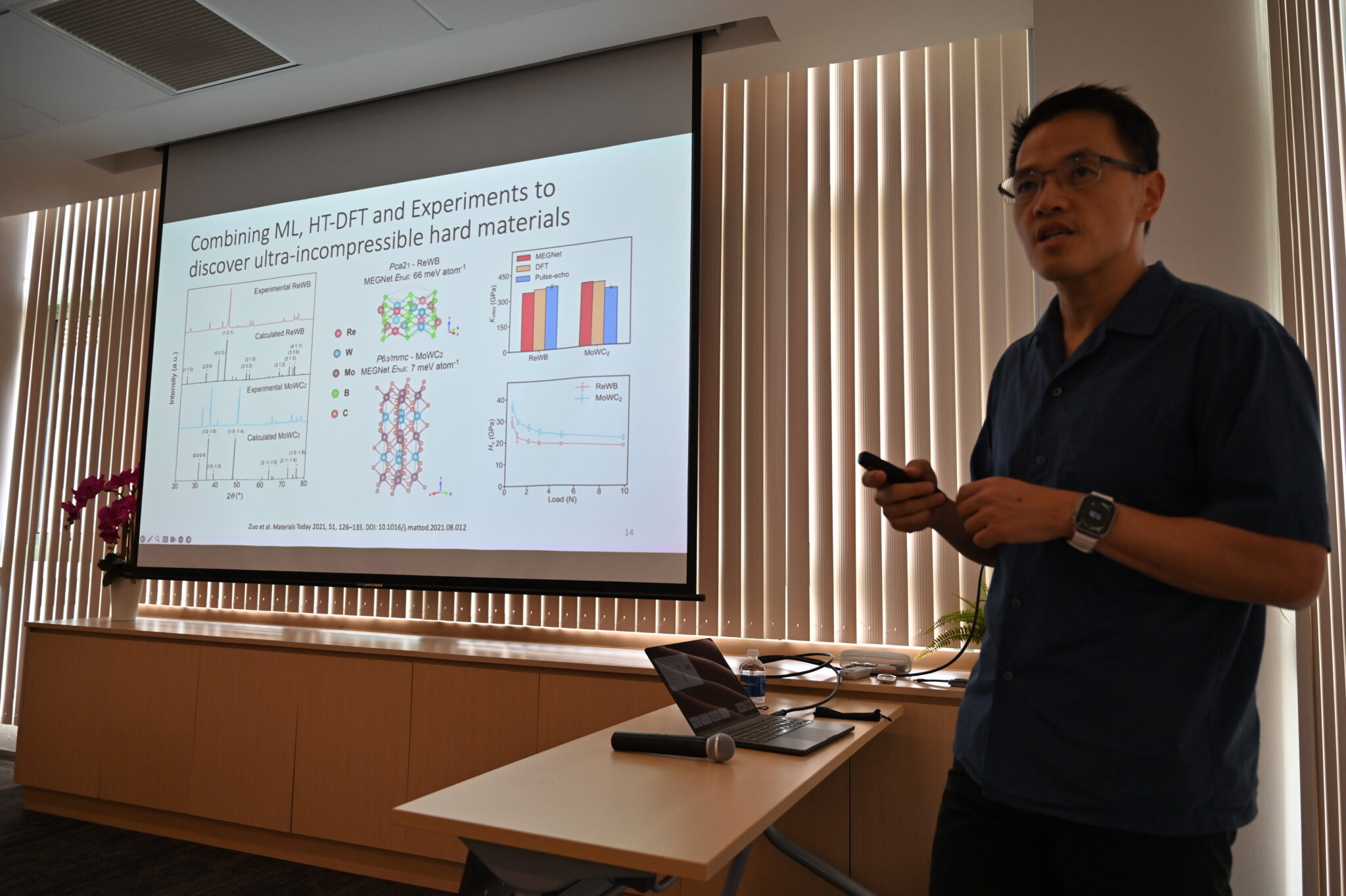
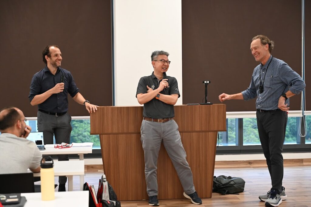
About the Professor: Prof Shyue Ping Ong is the Provost’s Chair Professor in Materials Science and Engineering at the National University of Singapore. He leads the Materialyze.AI lab, a materials informatics research group focused on the integration of materials science with data science and artificial intelligence to accelerate the discovery and design of materials. He is widely recognized as one of the pioneers of foundation potentials, i.e., machine learning interatomic potentials with comprehensive coverage of the periodic table that has broad applications in materials discovery and design. Prof Ong is also the founder and lead developer of pymatgen, one of the most popular open-source libraries for materials analysis, and a core contributor to the Materials Project, a public platform that provides computed properties of tens of thousands of inorganic compounds. Ong earned his PhD in Materials Science and Engineering from the Massachusetts Institute of Technology in 2011, and an MEng and BA in Electrical and Information Science from the University of Cambridge in 1999. He has authored more than 150 peer-reviewed publications, and has been recognized as a Clarivate Highly Cited Researcher since 2021. He is also a recipient of the prestigious US Department of Energy Early Career Research Program and the Office of Naval Research Young Investigator Program awards.
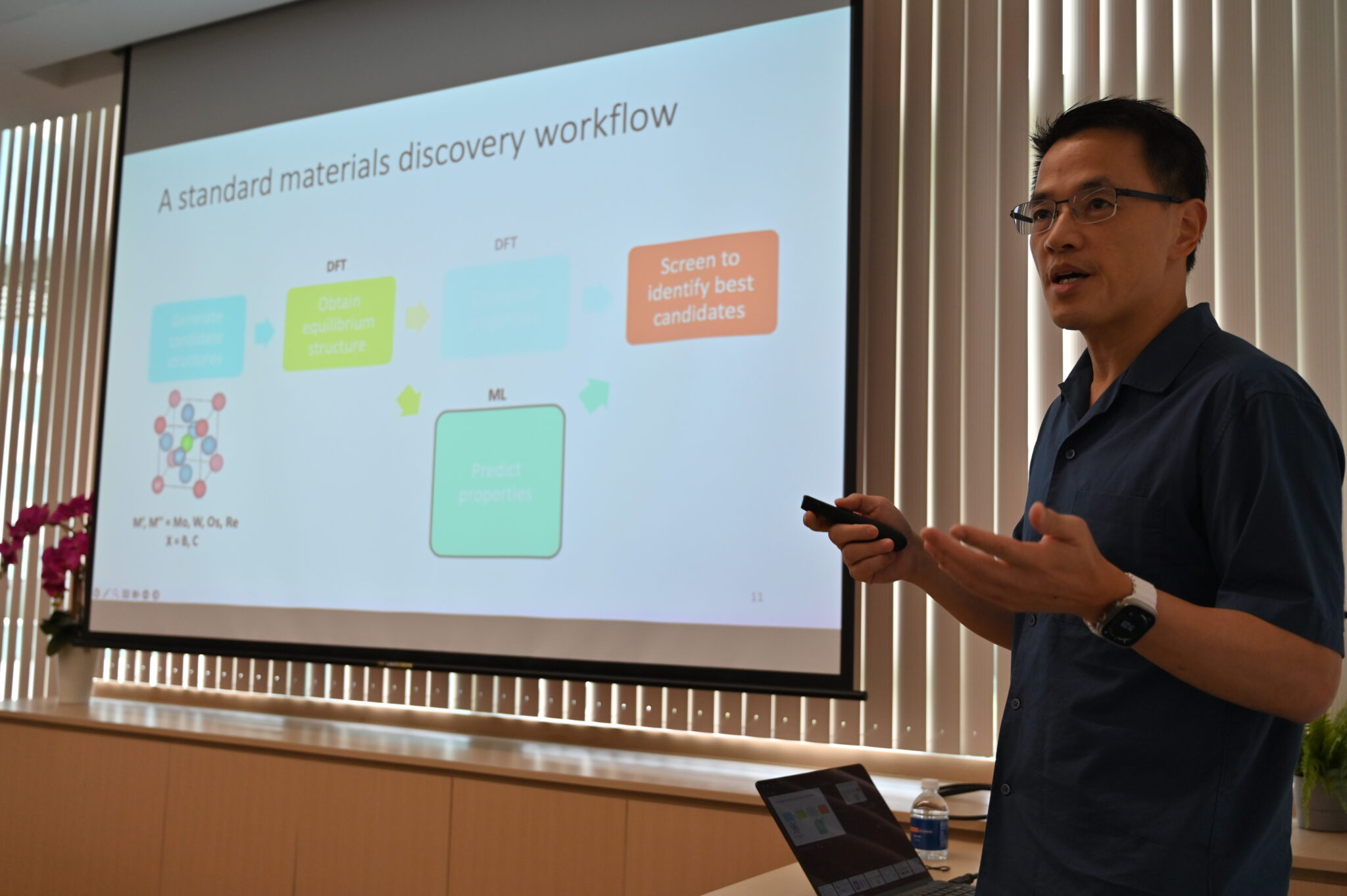
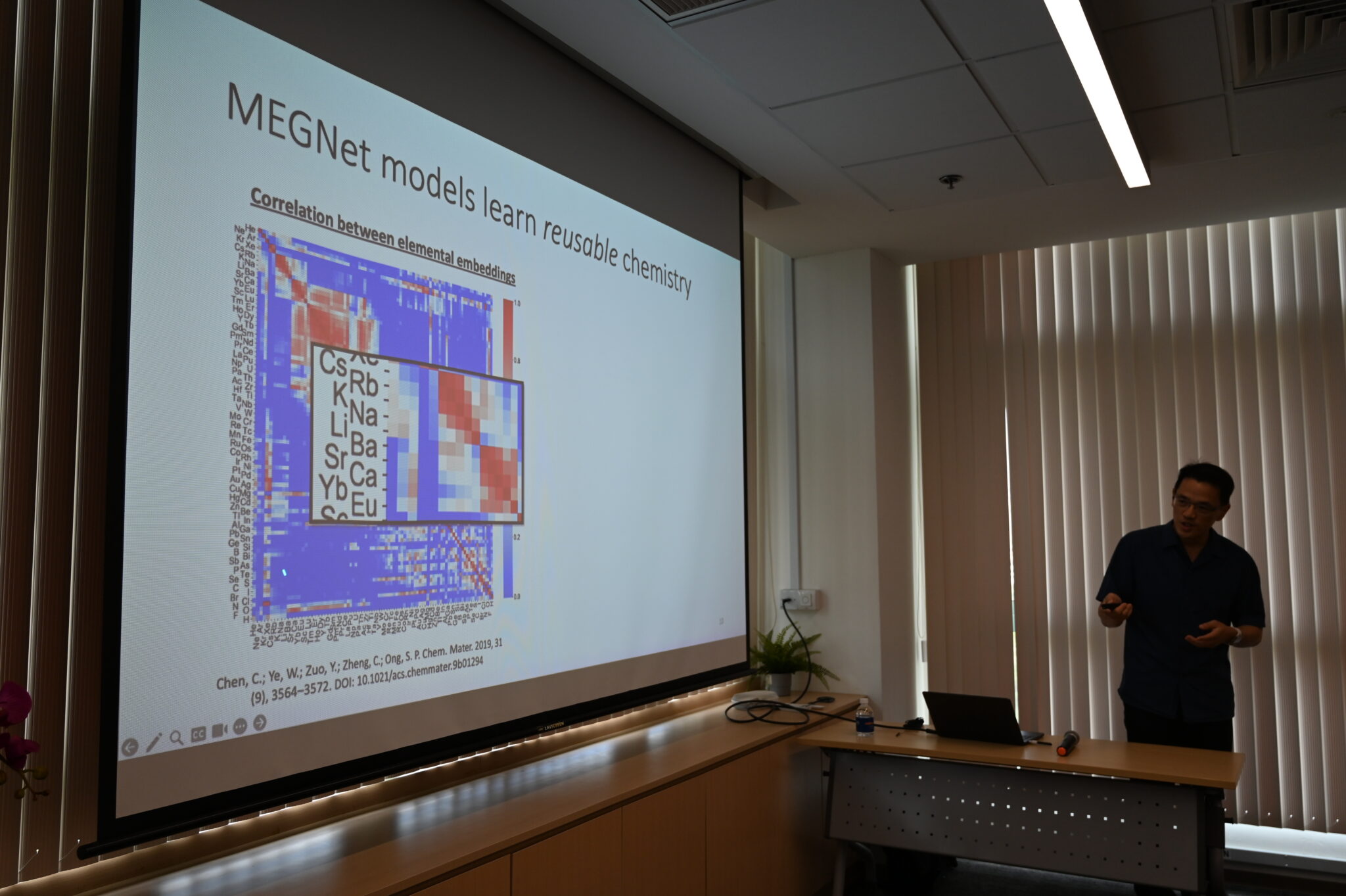
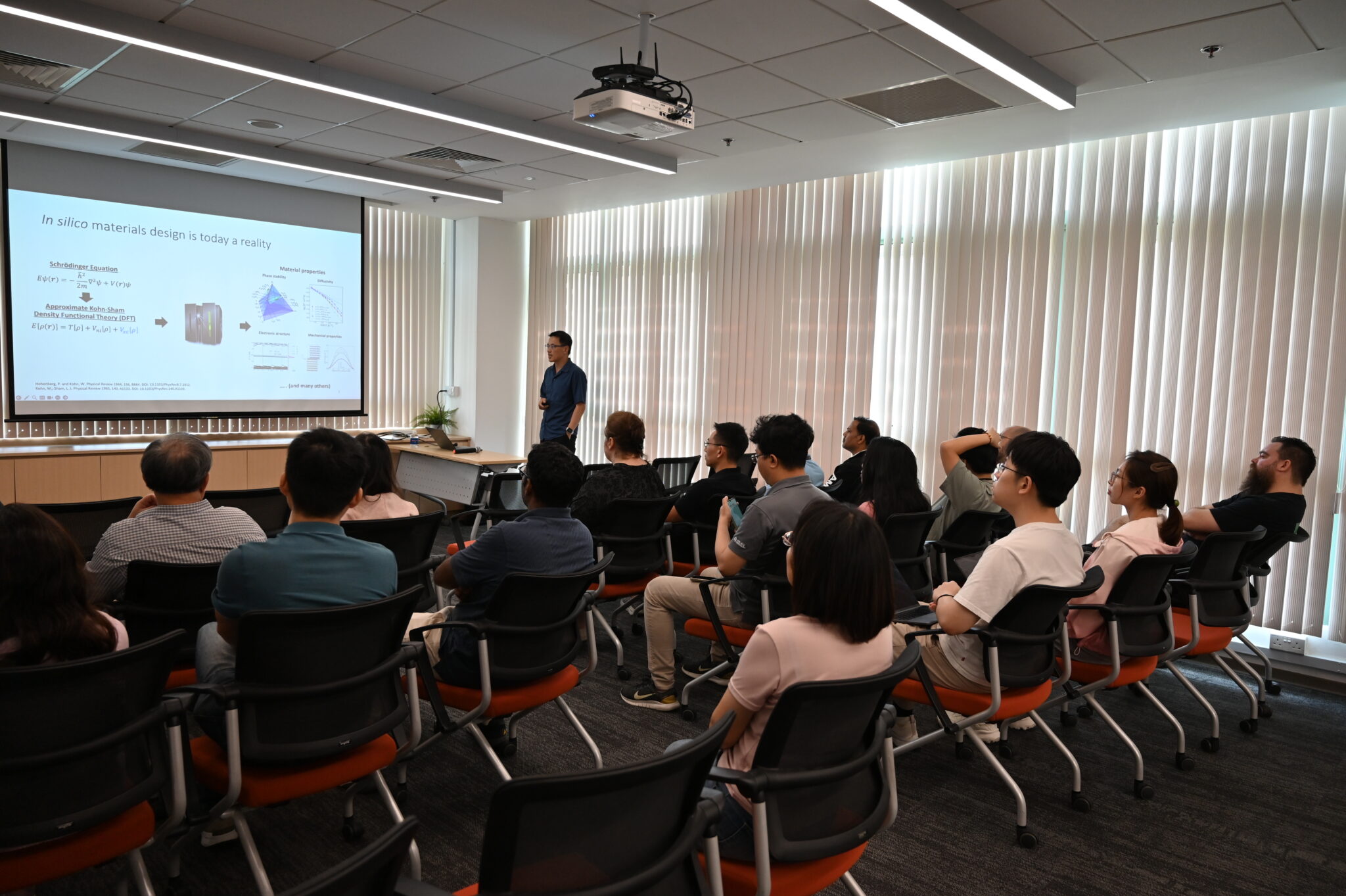
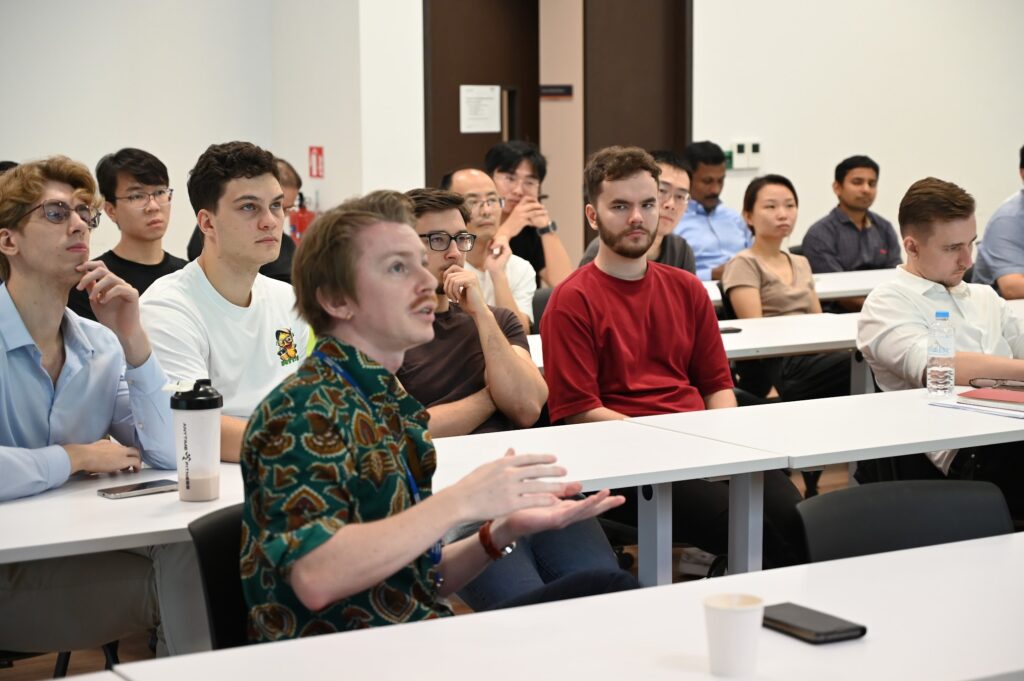
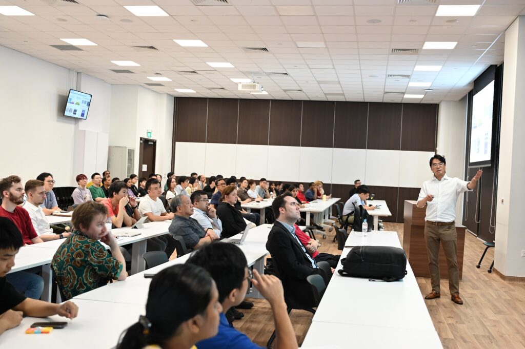
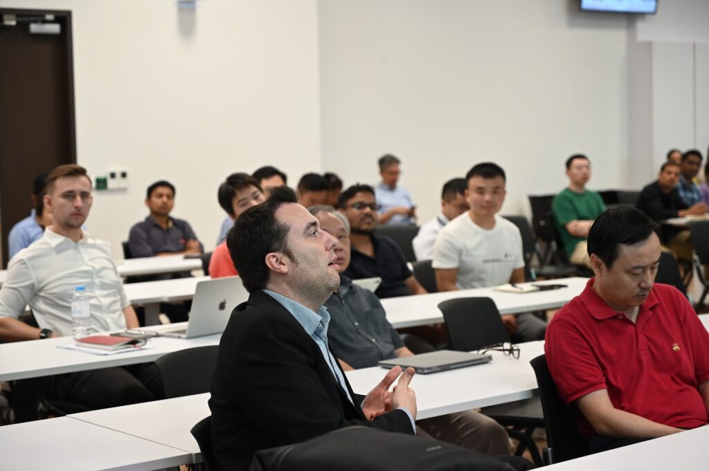
Abstract: Machine learning (ML) models have demonstrated human, or even superhuman, performance in many tasks, from playing traditional board games to image classification. In this talk, I will discuss how ML is having a similar transformative impact in materials science. Trained on large data sets, ML techniques can be used to discover novel technological materials as well as simulate complex systems at an accuracy beyond the reach of traditional computational techniques. A key focus of this talk will be on foundation potentials, which are universal interatomic potentials that have broad applications in structural relaxation, dynamic simulations, and property prediction of materials across diverse chemical spaces.
Date & Time: Wednesday, 21 January 2026, 12pm – 1.30pm.
Venue: Eureka Conference Room 1 & 2 (E6-06), NUS.
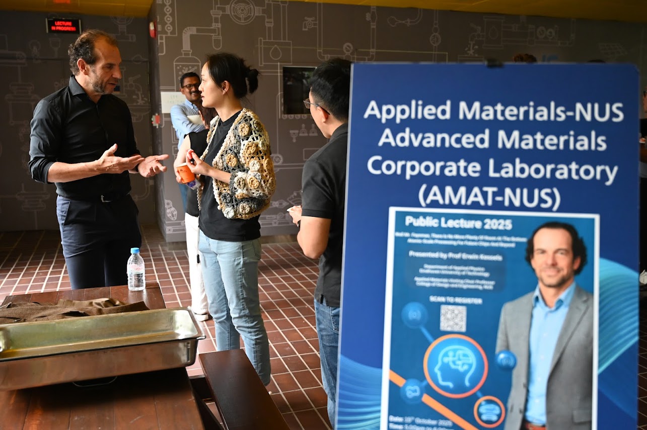
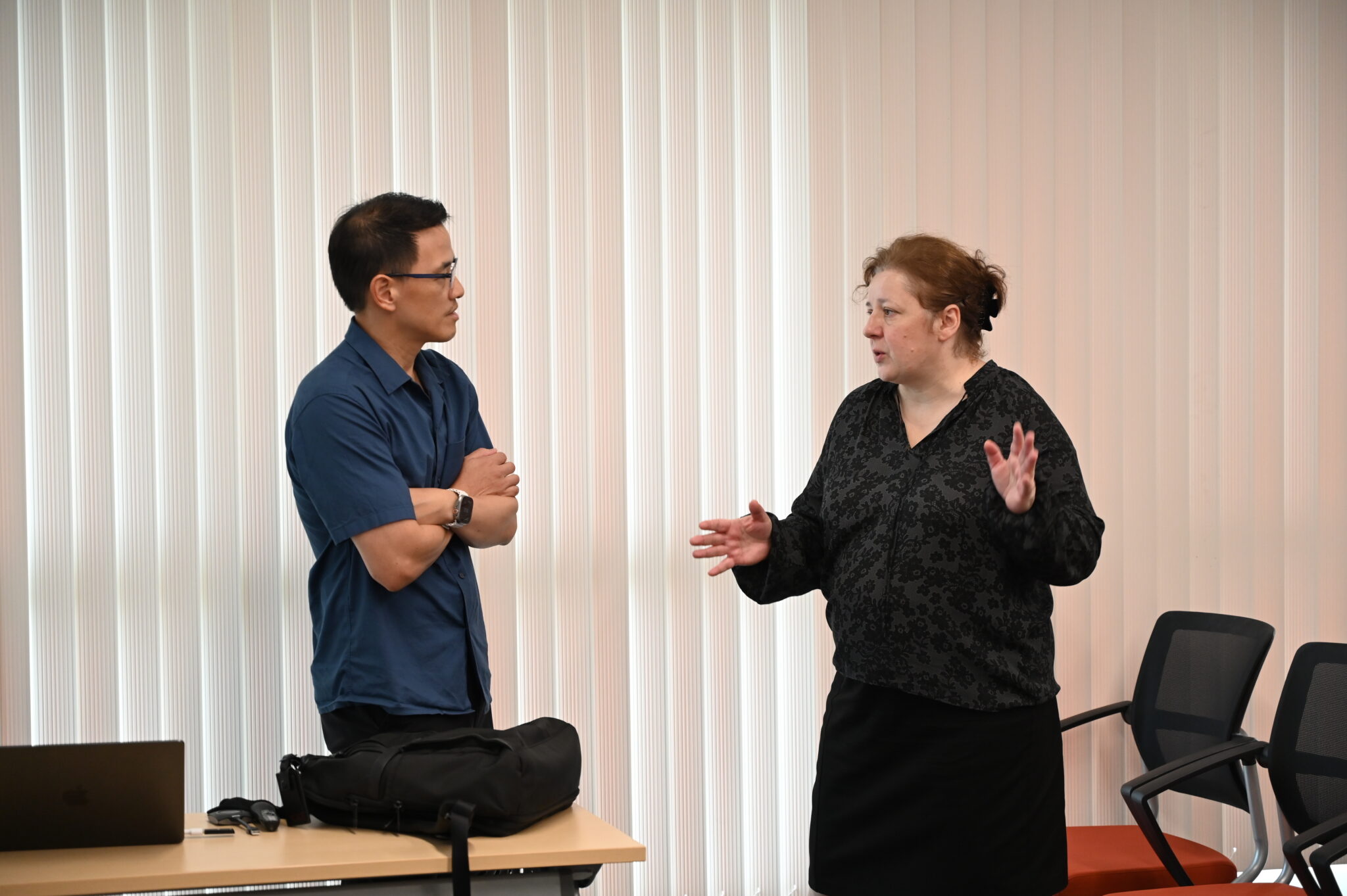
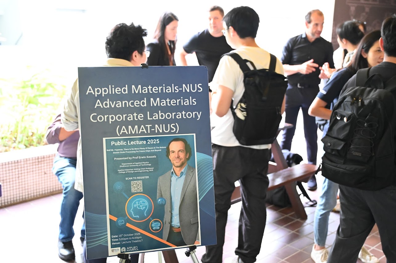
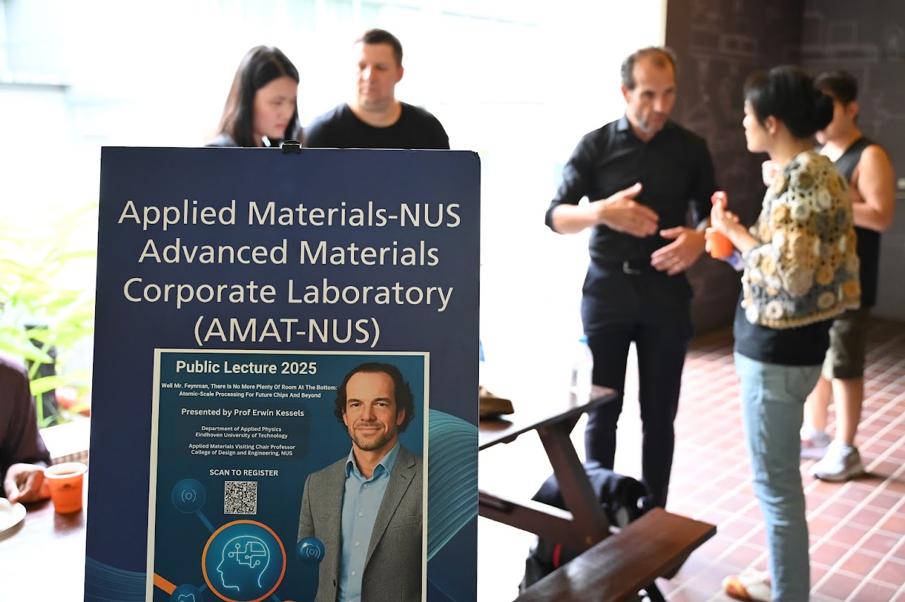
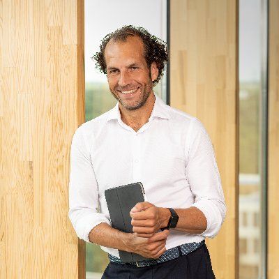
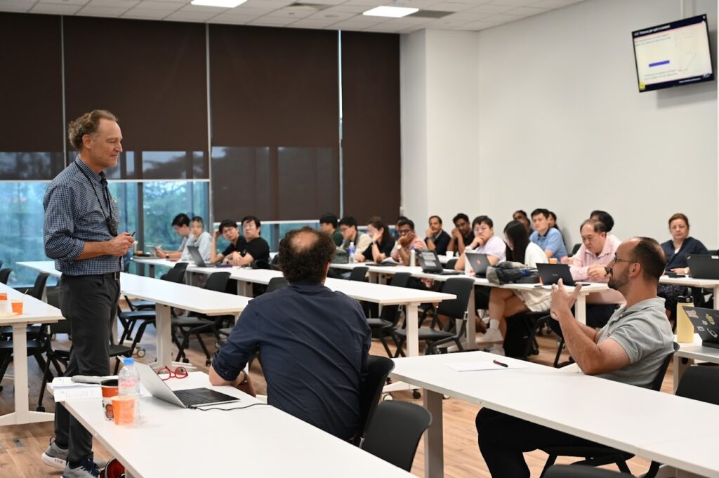
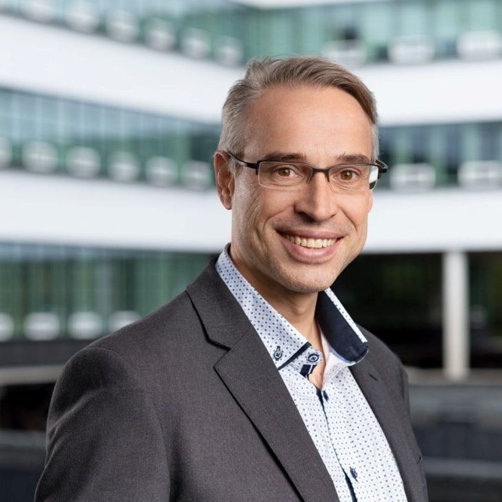
About the Professor: Prof. Erwin received his MSc (1996) and PhD (with honors) (2000) in Applied Physics from TU/e. His doctoral thesis work was partly carried out at the University of California Santa Barbara and as a Postdoc, he was affiliated to the Colorado State University and Philipps University in Marburg (Germany). In February 2025, he was appointed as an Applied Materials Visiting Professor under the AMAT Chair Professorship, in the Department of Materials Science and Engineering, College of Design and Engineering.
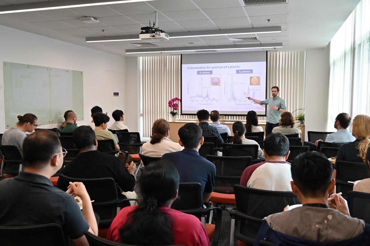
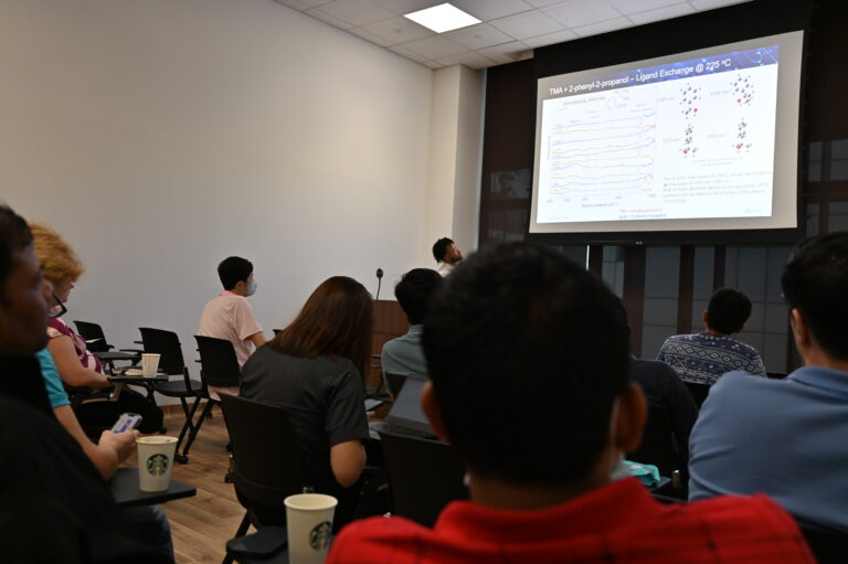
Topic 1: Plasma-surface interaction during atomic scale processing: Studying the reactive species coming to the surface Speaker: Gurp, Marnix Van, 2nd-year PhD candidate applying a variety of laser-based diagnostics to study plasma-surface interactions relevant to ALD and ALE. He also uses lasers for fundamental characterization of high-k stacks.
Abstract: Plasmas are essential in atomic-scale processes, such as: ALD, ALE, and surface treatments. However, it is often unclear which reactive plasma species are formed and delivered to the surface, limiting process control and physical understanding. In this talk, we report on our approach to measure fundamental plasma properties in our dedicated reactor using a variety of techniques, ranging from simple monitoring tools to advanced laser diagnostics.
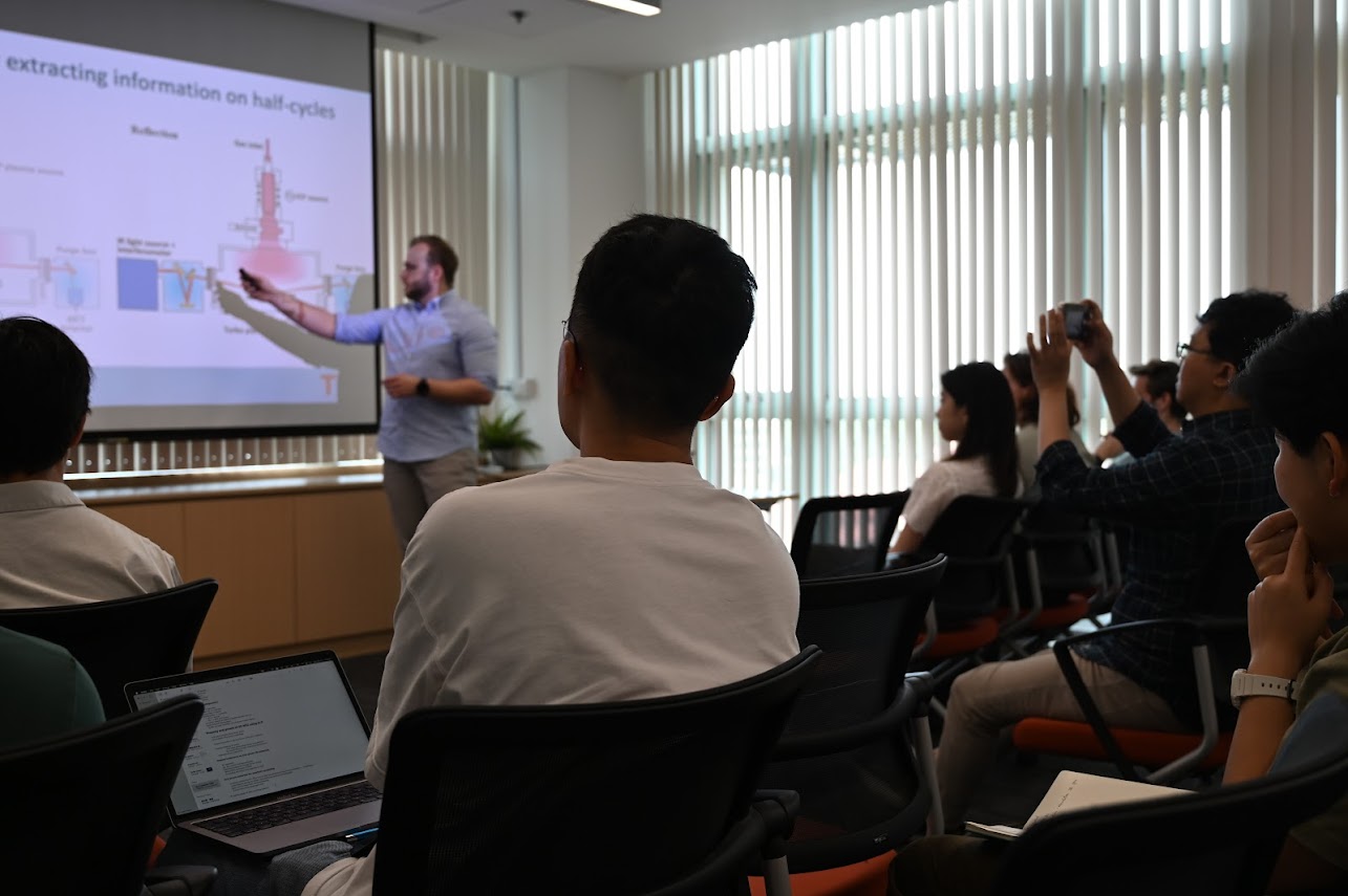
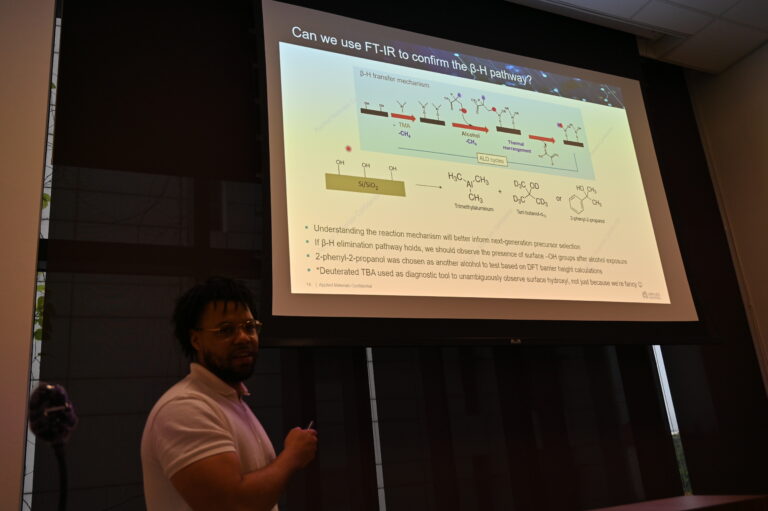
Topic 2: In-situ RAIRS for the investigation of the surface chemistry during half-cycles in ALD
Speaker: Werf, Sjoerd Van Der, 1st-year PhD candidate working on ALD of high-k dielectrics on graphene for CMOS compatible optoelectronic devices. Previously he worked with Applied Materials on ALD of low-k dielectrics for innerspacer fabrication for GAA-FET applications.
Abstract: The talk will mostly focus on the use of IR spectroscopy and more specifically reflection absorption infrared spectroscopy (RAIRS) as a diagnostic to gain information on the evolution of surface species during an ALD cycle.
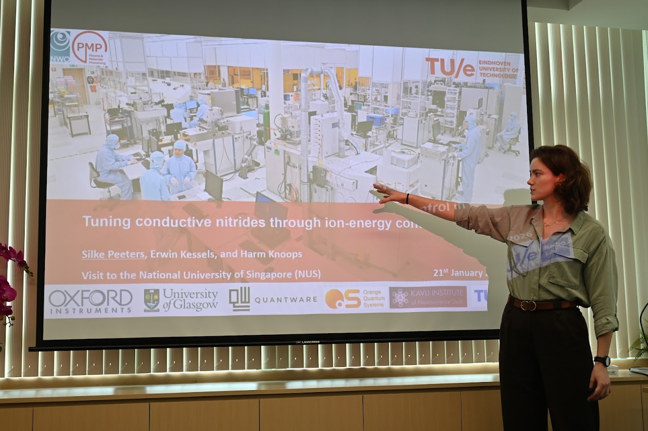
Topic 3: Tuning conductive nitrides through ion energy control in PEALD
Speaker: Peeters, Silke, 4th-year PhD candidate working on atomic layer deposition and etching of superconducting thin films, where she tailors the processes to the requirements of quantum technologies ranging from single-photon detectors to quantum bits.
Abstract: Thin films of conductive metal-nitride are key components in current and next-generation computing. The synthesis of conductive metal-nitride films on the nanometer-scale remains challenging. By controlling the ion-energy during plasma-enhanced atomic layer deposition, conductive films can be prepared at low temperature and short plasma exposure, and microstructure and composition can be tuned.
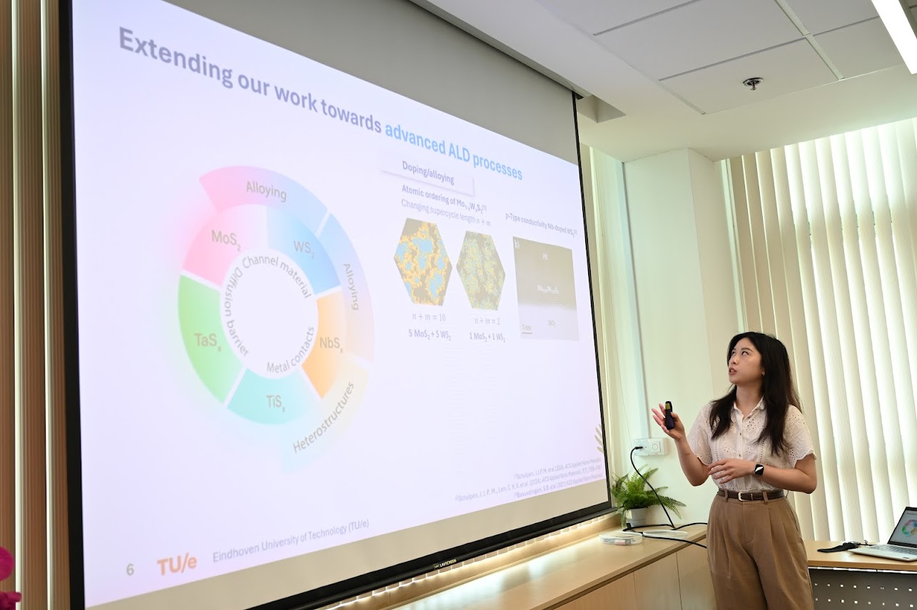
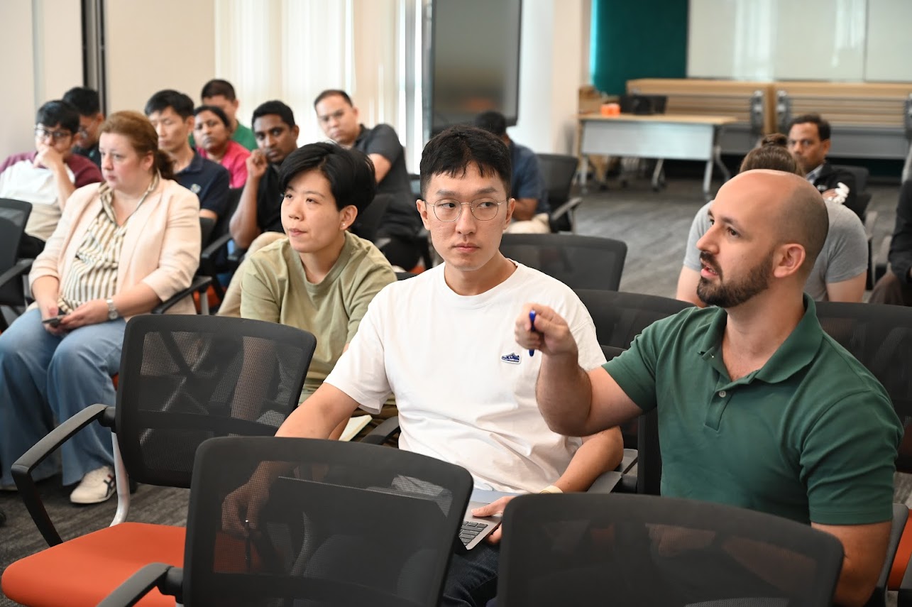
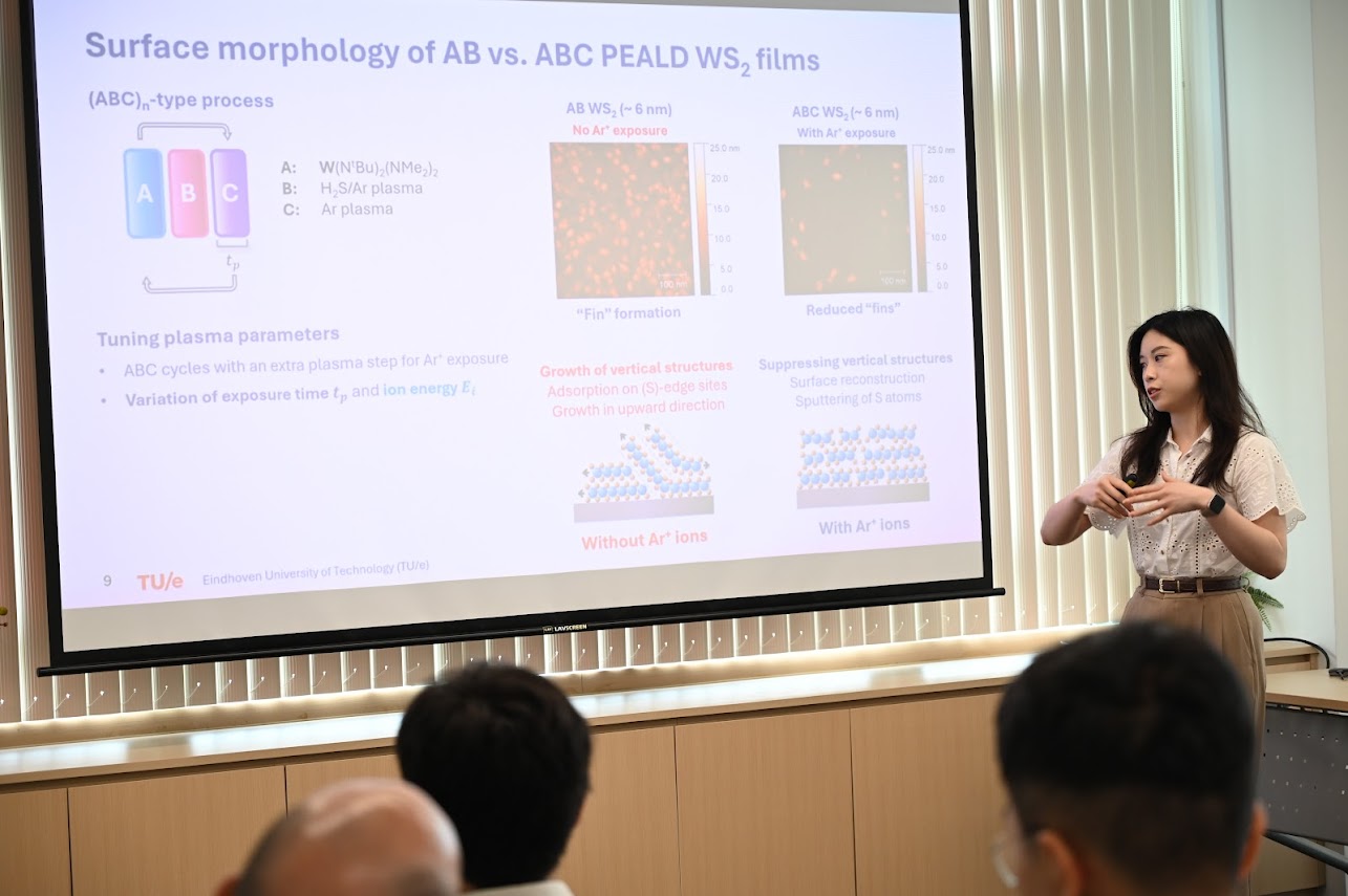
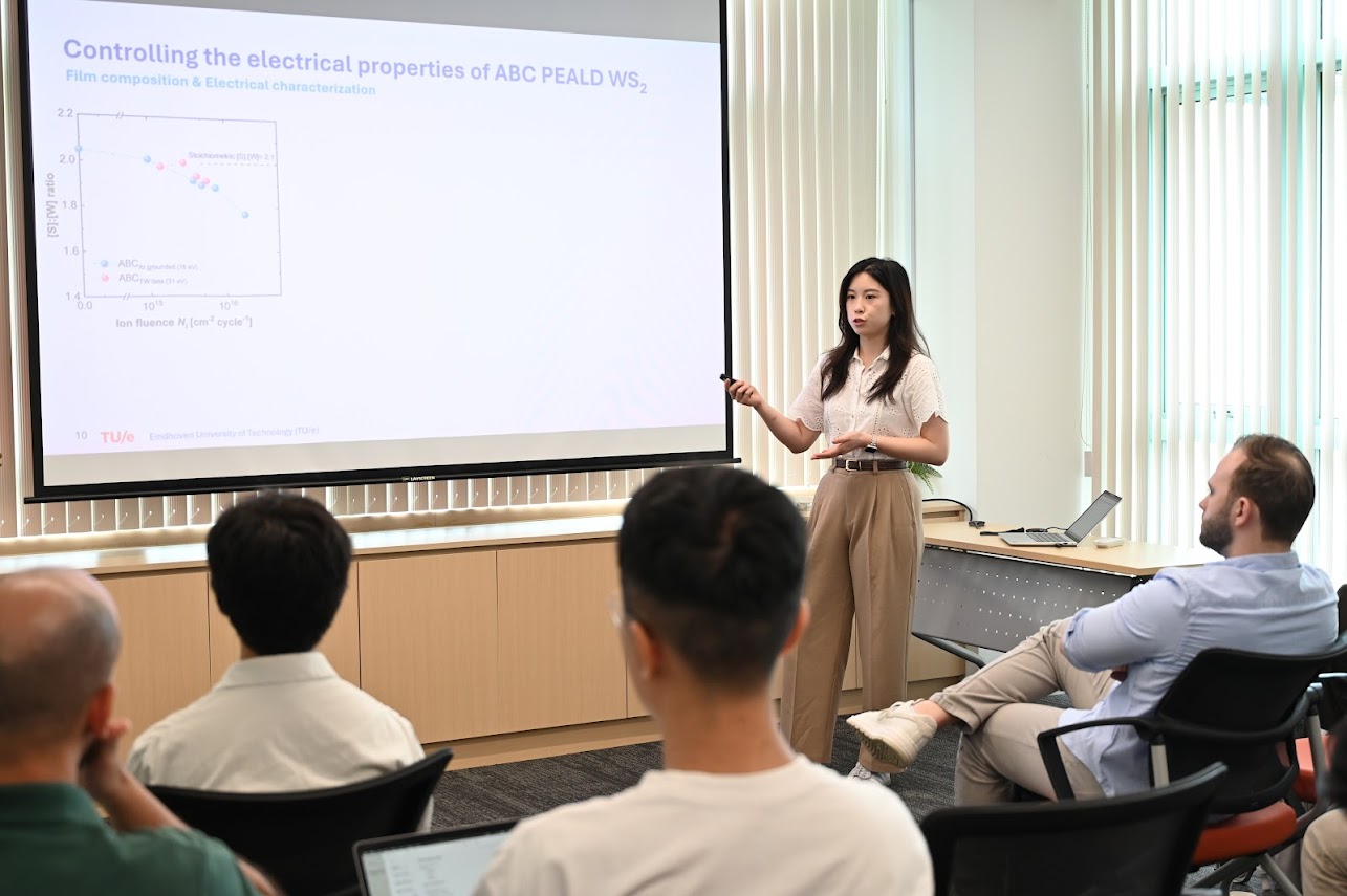
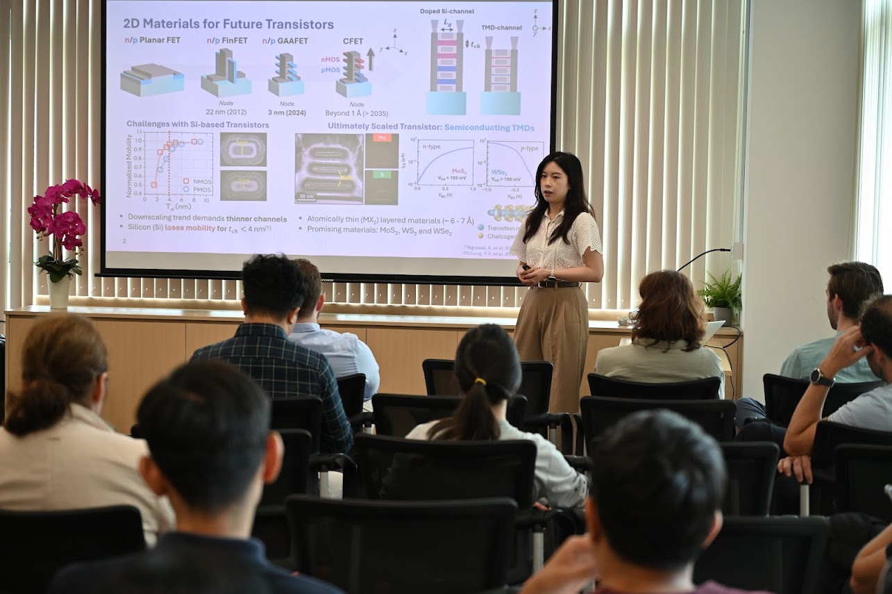
Topic 4: Beyond the conventional ALD process: Advanced approaches for controlling the properties and growth of WS₂ and MoS₂ 2D Materials
Speaker: Lam, Cindy, 3rd-year PhD candidate focusing on the growth of 2D TMDCs such as MoS₂ and WS₂ using advanced (plasma-enhanced) atomic layer deposition processes to tailor their material properties for nanoelectronic applications.
Abstract: As the semiconductor industry is progressing toward the Ångström era of transistor scaling, atomically thin 2D transition metal dichalcogenides (TMDCs) are potential future candidates to replace the current Si-based channel material in next-generation field-effect transistors (FETs). Atomic layer deposition (ALD) holds great promise as a deposition technique to grow 2D TMDCs directly on device-relevant substrates (i.e. transfer-free), conformal growth in 3D structures and back-end-of-line (BEOL) compatible temperatures. In this talk, I will present an overview of the ALD processes we have developed to establish a versatile library of TMDC materials (including MoS₂, WS₂, NbS₂ and TiS₂ ) and demonstrate how plasma (pre)treatments and supercycle approaches enable precise control over the film properties for targeted applications.
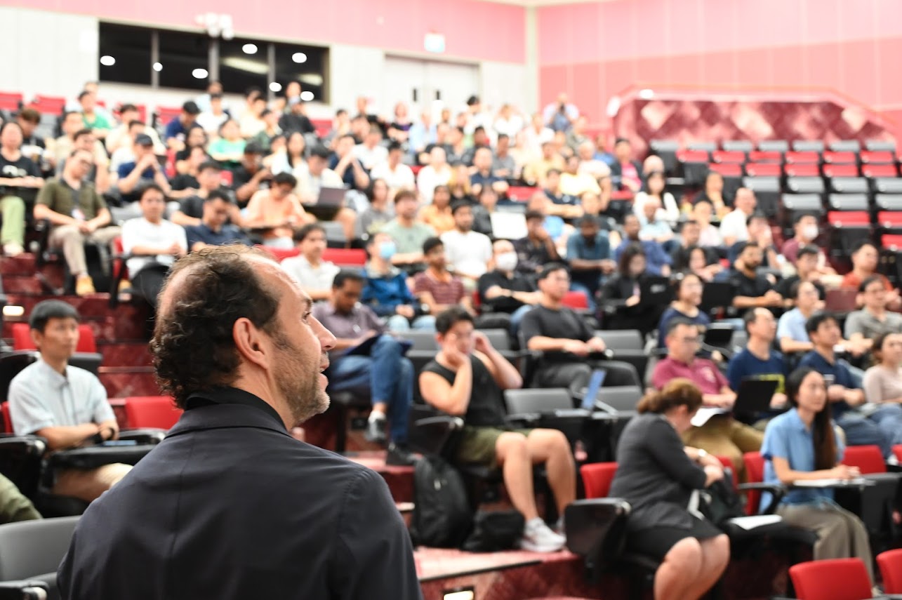
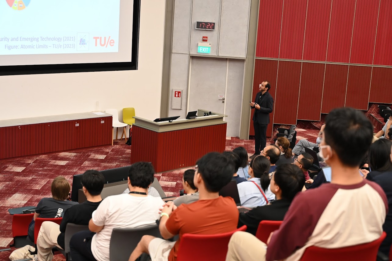
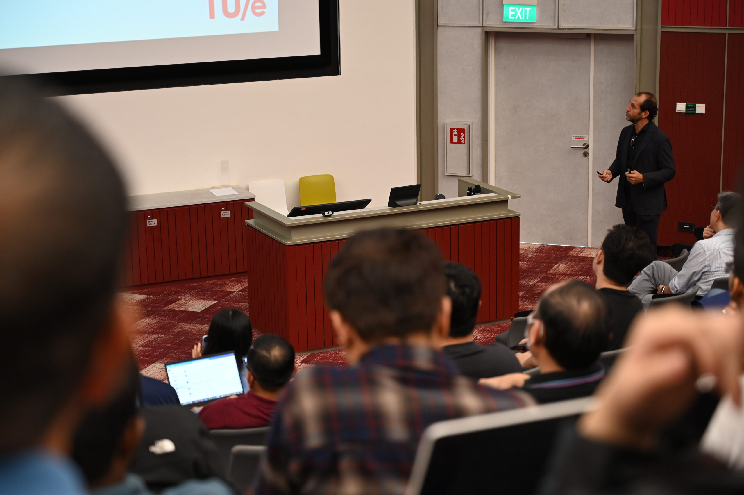
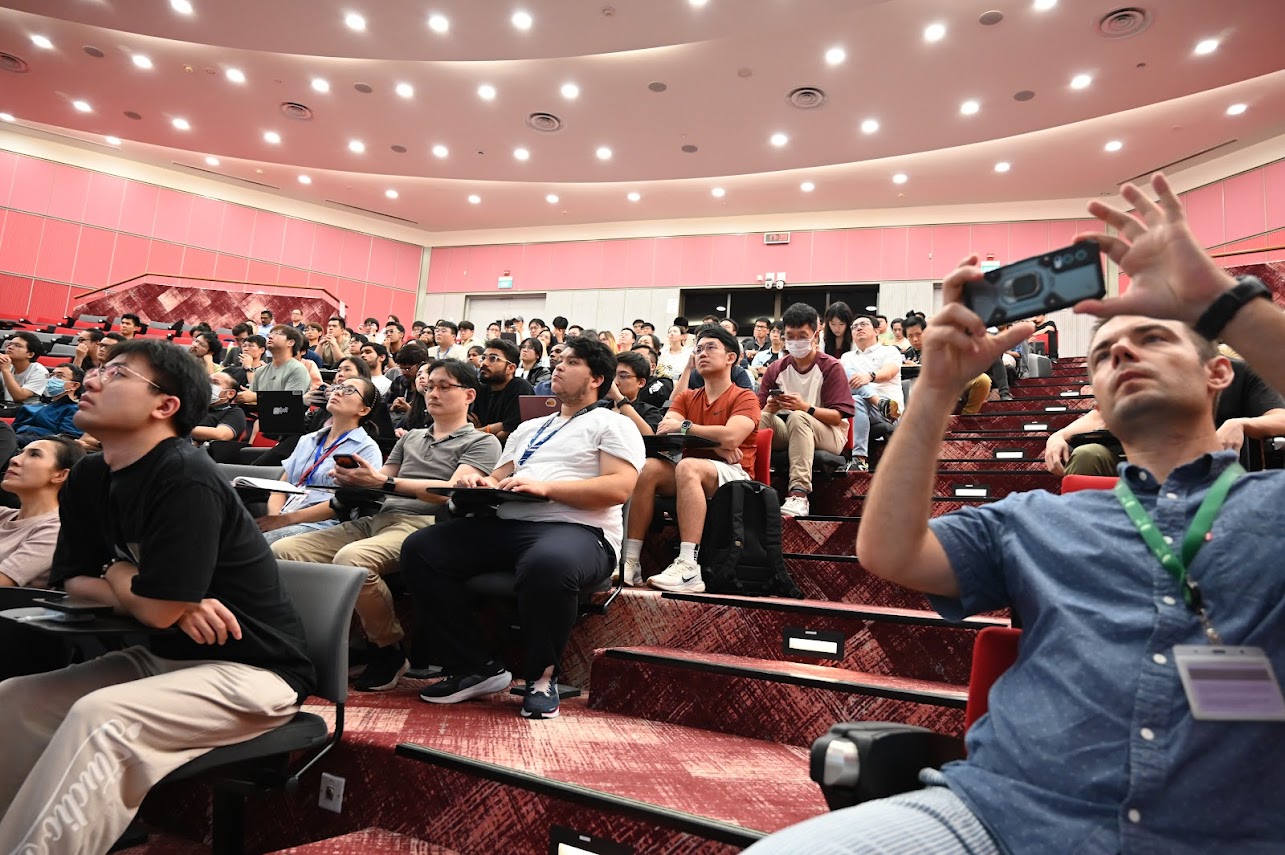
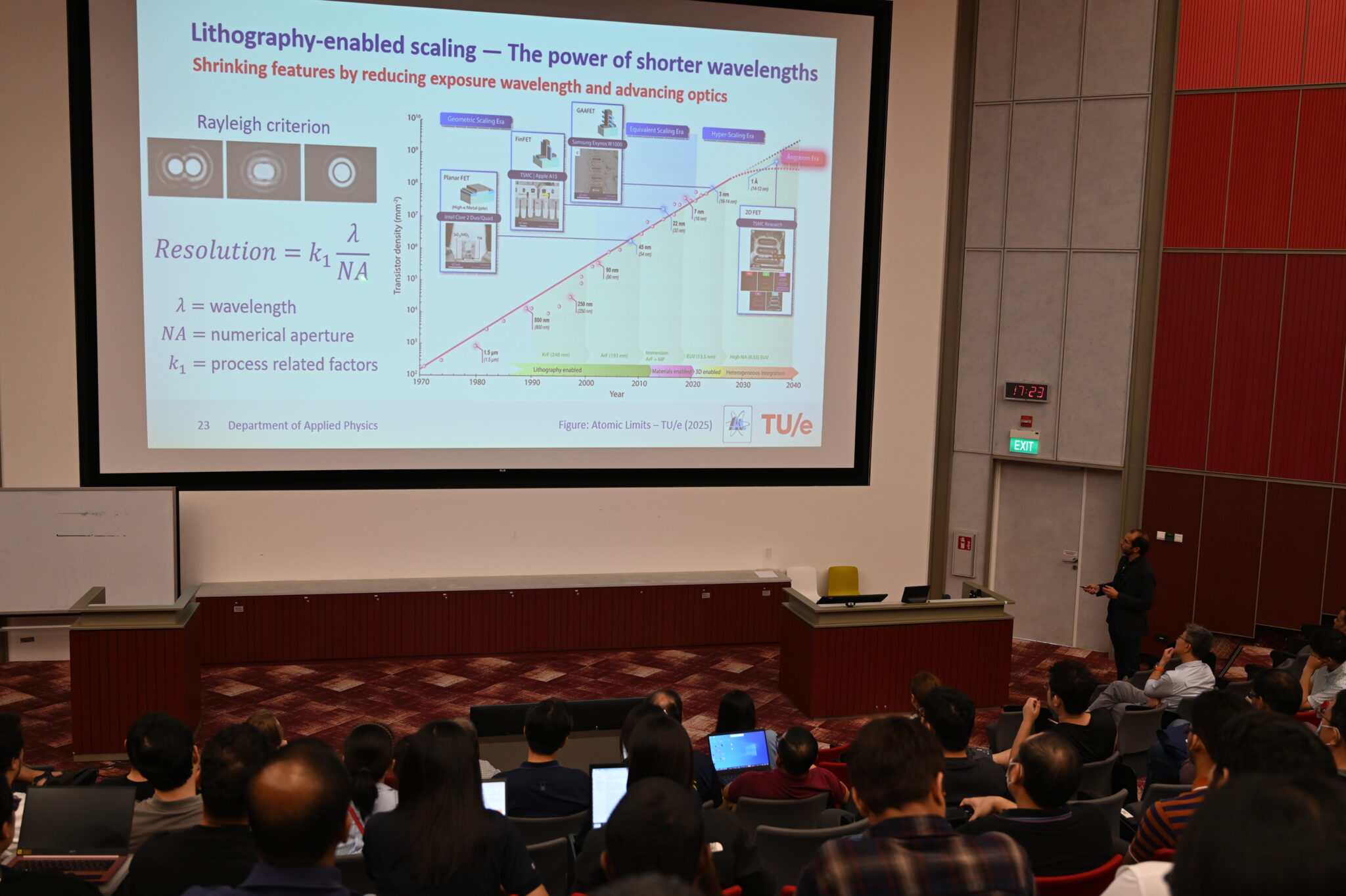
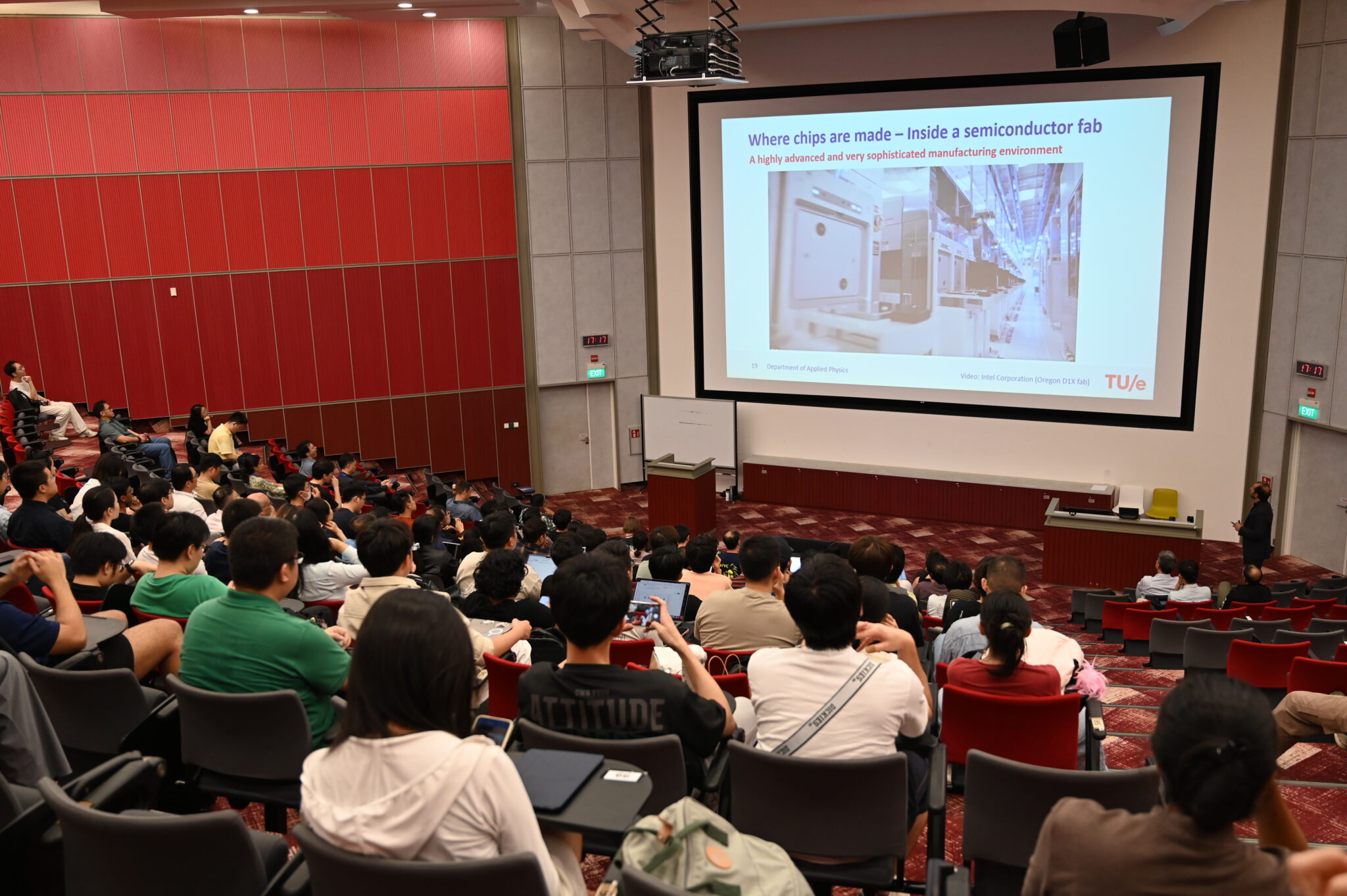
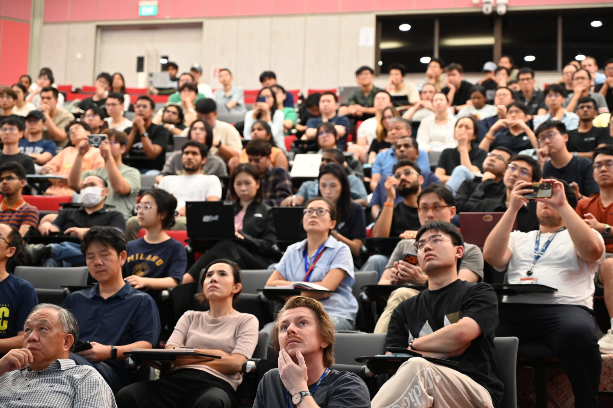
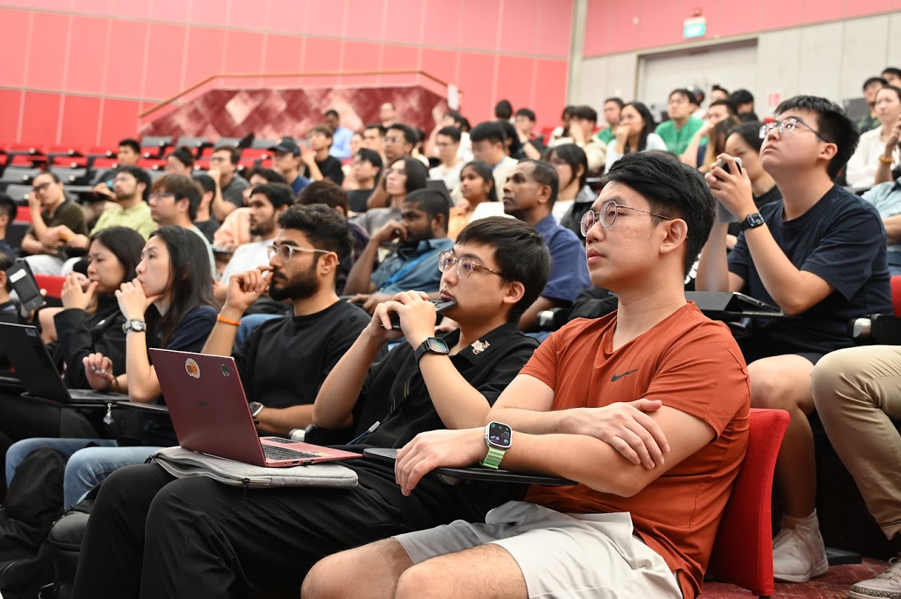
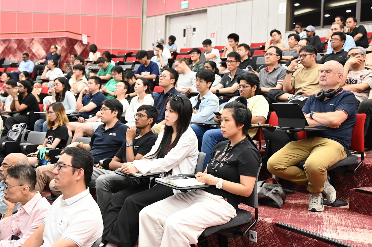
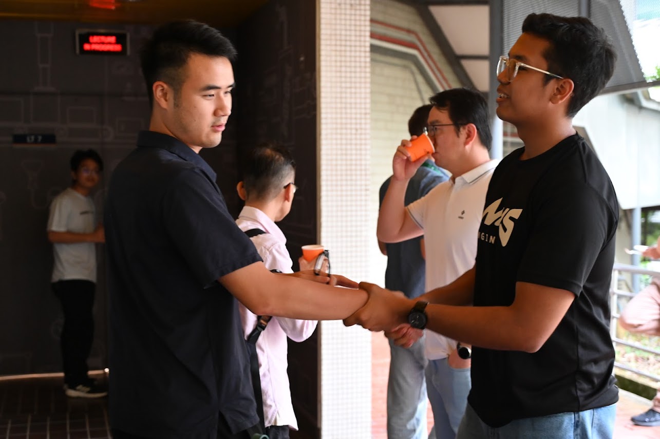
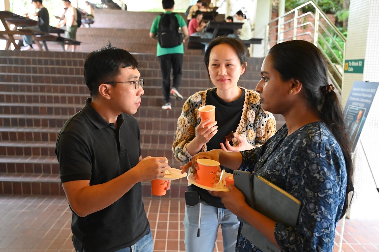
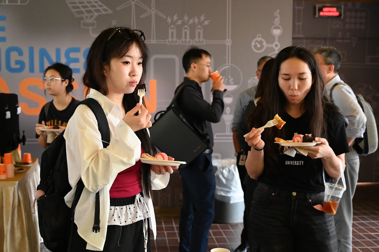
Date & Time: Wednesday, 15th October 2025, 5pm to 6pm
Venue: Lecture Theatre 7, EA Building, Level 3,
College of Design and Engineering (CDE), 9 Engineering Drive 1, NUS


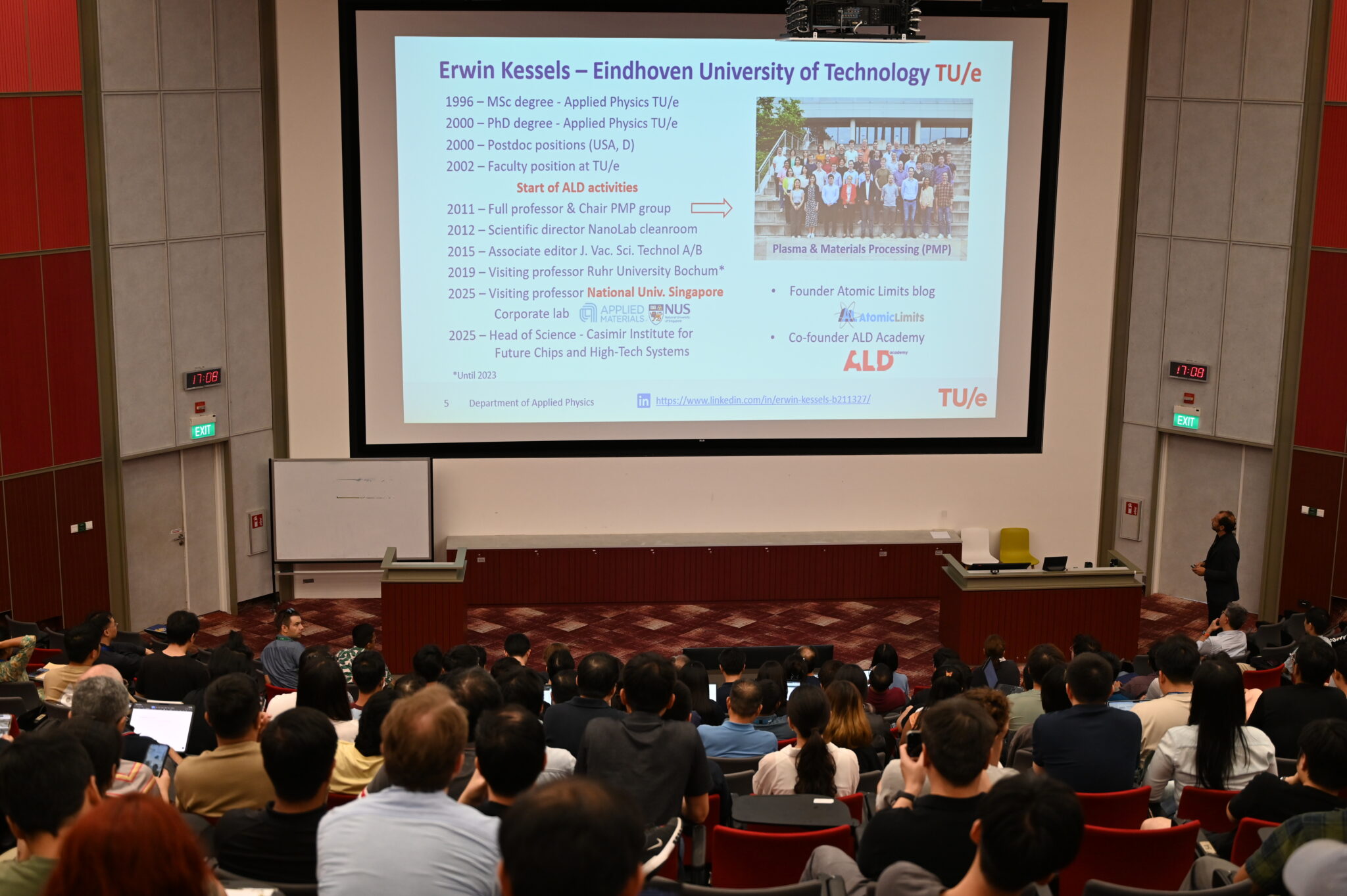


About the speaker: Prof. Erwin received his MSc (1996) and PhD (with honors) (2000) in Applied Physics from TU/e. His doctoral thesis work was partly carried out at the University of California Santa Barbara and as a Postdoc, he was affiliated to the Colorado State University and Philipps University in Marburg (Germany).
In February 2025, he was appointed as an Applied Materials Visiting Professor under the AMAT Chair Professorship, in the Department of Materials Science and Engineering, College of Design and Engineering.
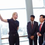
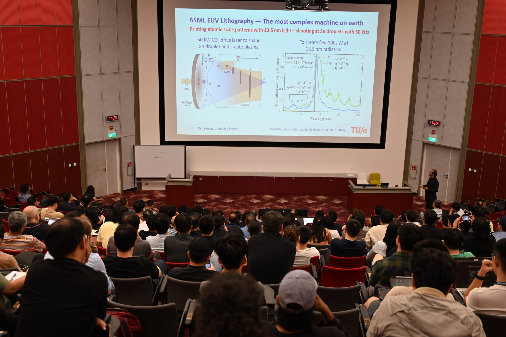
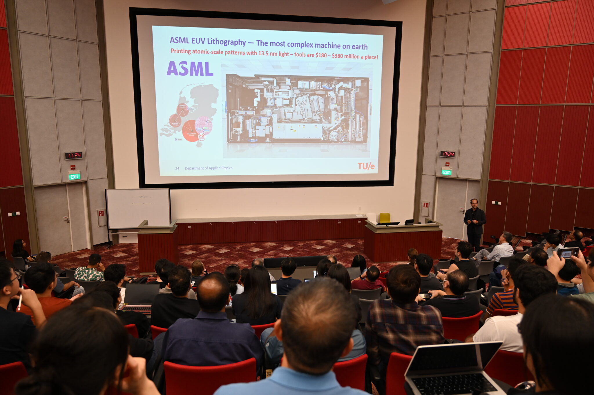
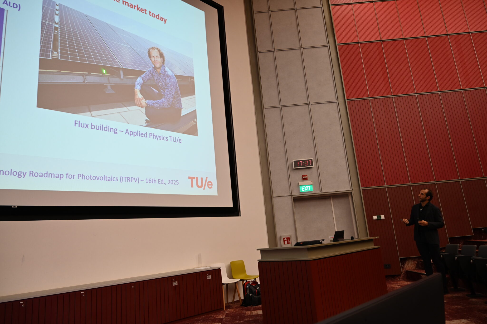
Abstract: In his famous 1959 lecture “There’s Plenty of Room at the Bottom,” Richard Feynman suggested that extraordinary progress could be achieved by scaling things down. For decades, this vision guided the semiconductor industry under Moore’s Law. Today, however, the “plenty of room” has largely been used up. Further advances now rely on highly sophisticated processing methods, where atomic precision — also foreseen by Feynman — has become indispensable.
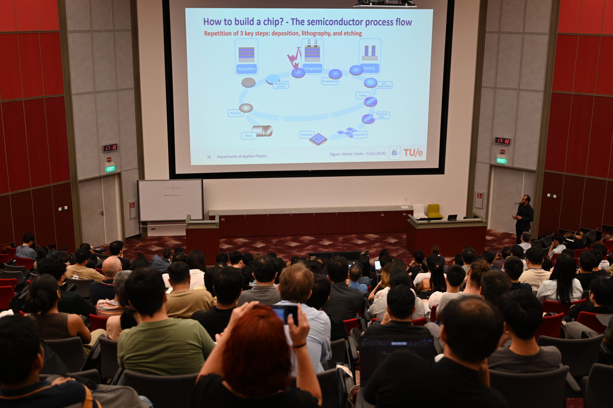
Extreme ultraviolet lithography, enabled by the most complex high-tech systems on Earth, defines patterns at the smallest dimensions. Deposition and etching of materials atomic layer by atomic layer, combined with selective processing at defined locations, provide the atomic-scale control needed to build nanoscale patterns. Together, these approaches enable the fabrication of highly complex three-dimensional device architectures that underpin future logic and memory technologies. Beyond semiconductors, the same methods are increasingly applied in energy conversion and storage, where thin-film precision is equally critical.


Date & Time: Tuesday, 5th August 2025, 11am to 12pm
Venue: Building E7, Seminar Room 4 (#E7-03-09)
About the speaker: Prof. Yi Hou is a Presidential Young Professor in the Department of Chemical and Biomolecular Engineering at the National University of Singapore (NUS). He leads the Perovskite-based Multijunction Solar Cell Group at the Solar Energy Research Institute of Singapore (SERIS). His research focuses on advancing perovskite photovoltaics, particularly in tandem solar cell architectures. Prof. Hou has authored over 100 high-impact publications in Science, Nature, Nature Energy, and related journals, accumulating more than 14,000 citations. He has been recognized as a Clarivate Highly Cited Researcher (2022–2024) and was named an MIT Technology Review Innovator Under 35 (Asia Pacific). He also serves as an Editor for the IEEE Journal of Photovoltaics. In addition to his academic and editorial roles, Prof. Hou is the founder of Singfilm Solar, a leading NUS spin-off company commercializing perovskite solar cell technology, with a pilot manufacturing line established in Singapore.
Abstract: Perovskite solar cells (PSCs) have emerged as a leading next-generation photovoltaic technology, demonstrating strong potential both as single-junction devices and in tandem configurations with silicon and other absorbers. Despite recent certified efficiencies exceeding 25.7% for 1 cm² devices, challenges such as interface recombination and long-term stability still hinder large-scale adoption. This talk will discuss strategies to overcome these limitations through advanced interface engineering and material design. Emphasis will be placed on the development of wide-bandgap perovskites and their integration into high-efficiency tandem systems, including record-setting combinations: Perovskite/Organic (30.0%), Perovskite/CIGS (30.0%), Perovskite/Silicon (33.4%), and Perovskite/Perovskite/Silicon triple-junctions (30.0%). The presentation will conclude with perspectives on commercialization and the role of perovskite-based tandems in the future PV landscape.

Date: March 4-5, 2025
Venue: Building E7, Seminar Room 4 (#07-03-09)
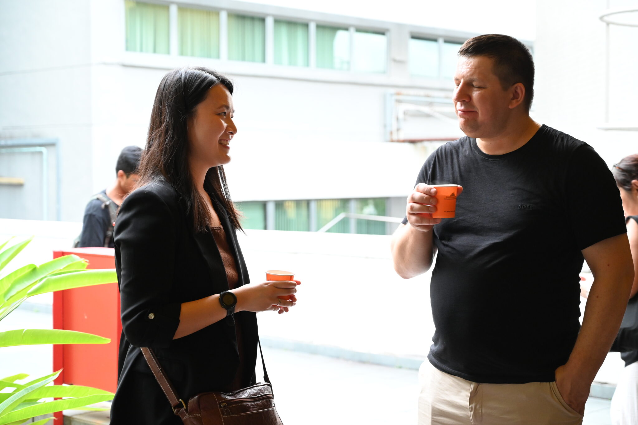
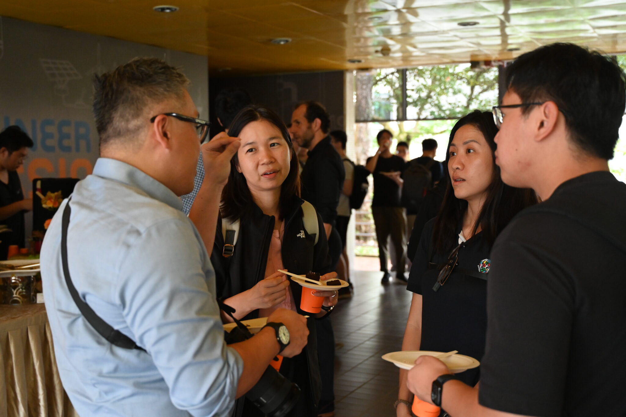
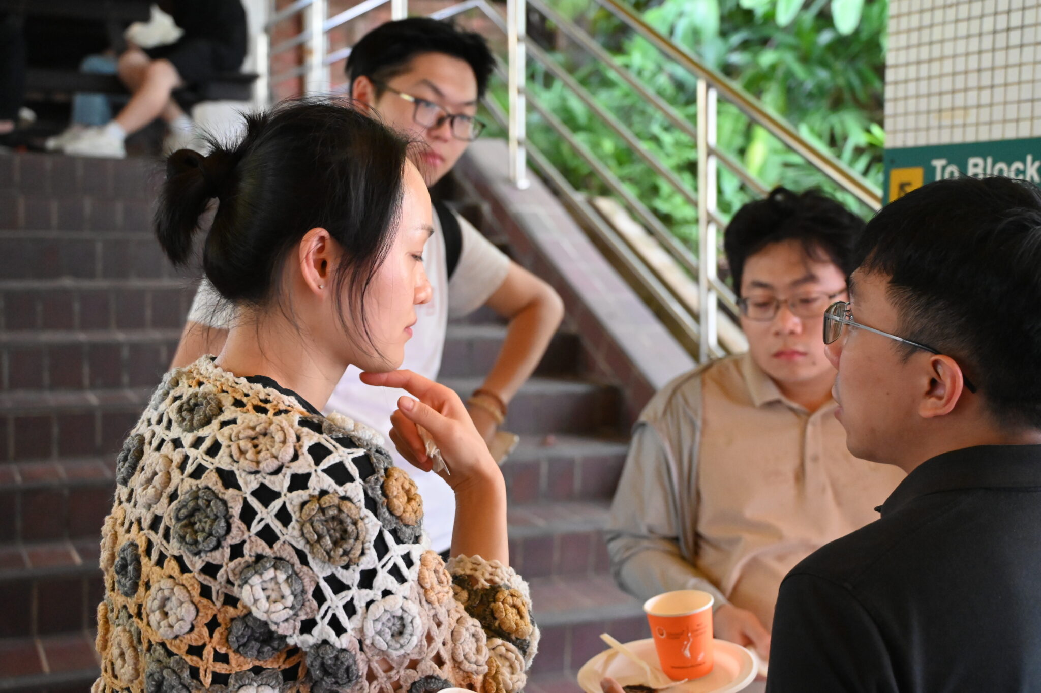
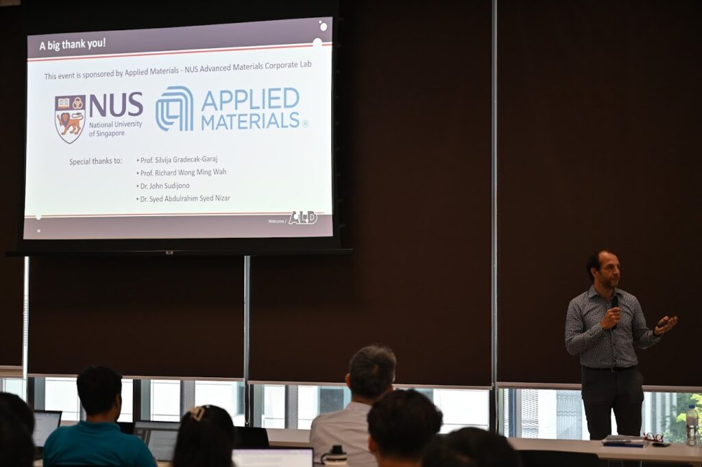
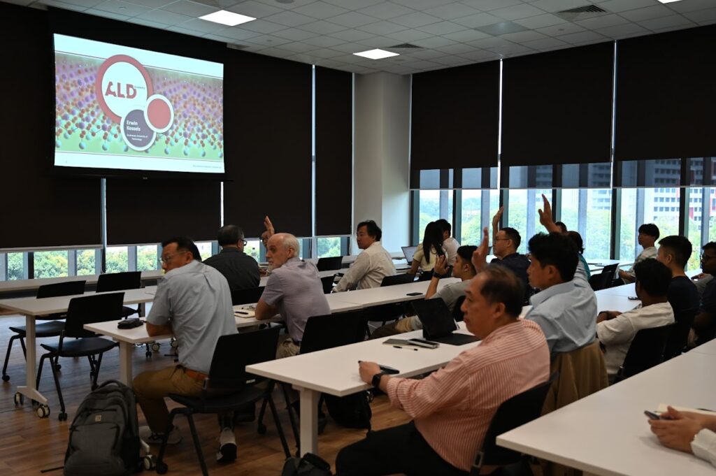
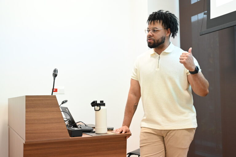
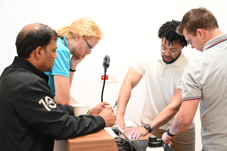
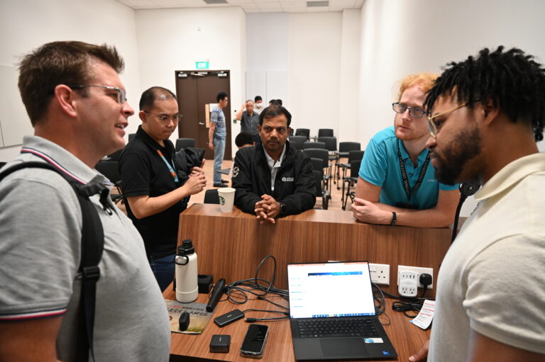
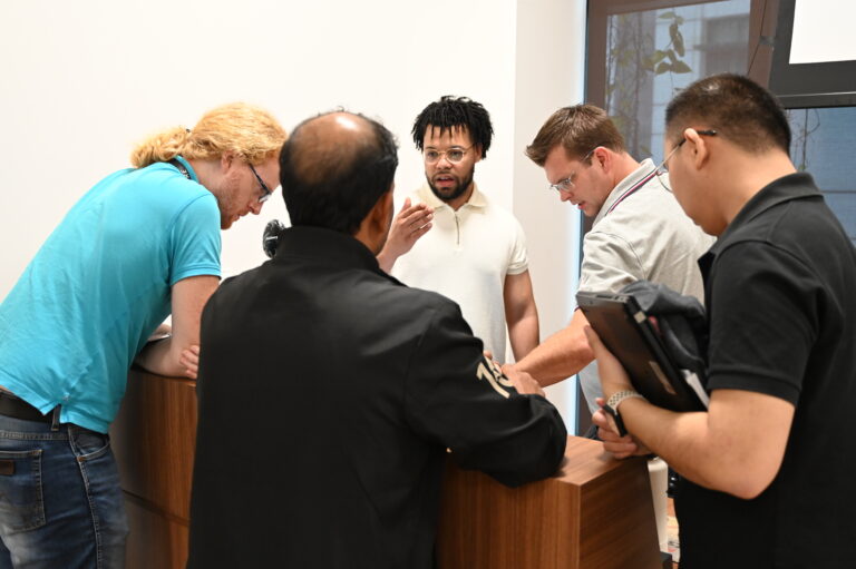
The Applied Materials – NUS Advanced Materials Laboratory hosted the ALD Academy 2025 workshop which offered an exciting opportunity for a deep dive into atomic layer deposition (ALD) techniques and their diverse applications across various fields. This two-day event had introduced participants to ALD as a key atomic-scale processing method, covering essential topics such as ALD fundamentals, processes, and applications. It served as an invaluable chance for even members of the public to be part of a forward-thinking community at the forefront of ALD research and development!
Designed for both newcomers and professionals alike, this workshop had been ideal for anyone looking to build a stronger foundation in ALD and related atomic-scale processing techniques. This unique opportunity allowed our participants to gain advanced insights, exchange ideas, and collaborate with experts in the field. Participants enhanced their understanding of cutting-edge ALD technologies and their potential to drive innovation in materials science.
About The Speakers:
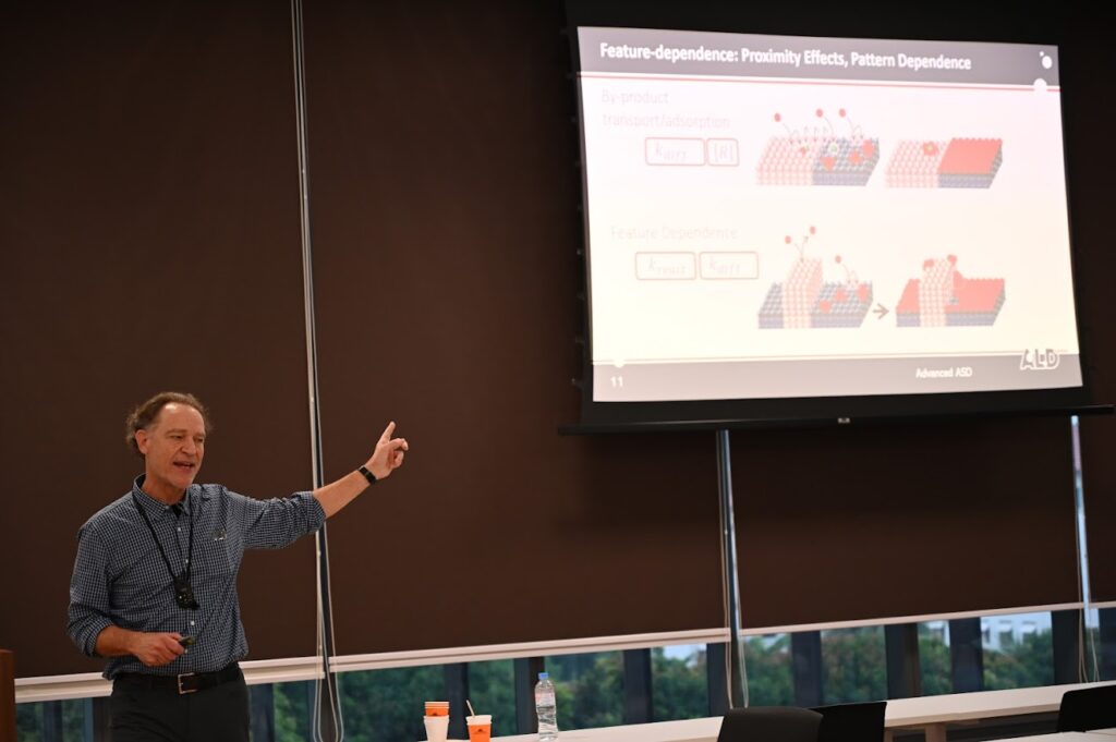
1. Prof. Erwin Kessels – Eindhoven University of Technology, Netherlands (Top Photo)
Erwin received his MSc (1996) and PhD (with honors) (2000) in Applied Physics from TU/e. His doctoral thesis work was partly carried out at the University of California Santa Barbara and as a Postdoc he was affiliated to the Colorado State University and Philipps University in Marburg (Germany).
In 2004/2005 he spent six-months sabbatical at the University of California Berkeley. In 2007, the American Vacuum Society awarded him the Peter Mark Memorial Award. Erwin received an NWO Vici grant in 2010 to set up a large research program on ‘nanomanufacturing’ to bridge the gap between nanoscience/nanotechnology and industrial application. In 2008 he was chair of the International Conference on Atomic Layer Deposition in 2008 (Bruges, Belgium) and in 2019 he received the ALD Innovator award at this yearly conference. Erwin will serve as a chair of the 7th workshop on atomic layer etching in 2020 (Ghent, Belgium). Since 2019 Erwin has also been appointed as Visiting International Professor and a DFG Mercator fellow at the Ruhr University Bochum. Erwin is active within the American Vacuum Society and has been President of the Netherlands Vacuum Society. He is an associate editor of the Journal of Vacuum Science and Technology. He has published over 300 papers, has given 100+ invited presentations, and holds 4 patents. He frequently co-organizes ALD-related workshops and is the founder of the ALD Academy and the blog AtomicLimits.com.
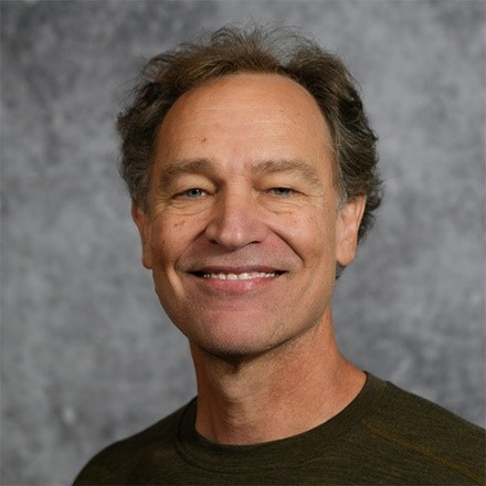
2. Prof. Gregory Parsons – North Carolina State University, U.S.A. (Bottom Photo)
Parsons’ research explores chemical reactions on surfaces, particularly for formation of thin films by atomic layer deposition. He joined the faculty at NC State in 1992, after a Postdoc position at IBM TJ Watson Research Center. His research interests include Atomic Layer Deposition and related processes; Physics of Electronic Materials and Devices; Polymer Fiber and Film Formation, Coating and Chemical Surface Modification; Metal-Organic-Framework (MOF) Materials and Thin Films; Advanced Energy Storage and Solar Energy Conversion. His expertise also includes: Thin Film Transistor(TFT) and Flat Panel Active Matrix Display (esp. AMLCD) Devices and Manufacturing, Chemical Vapor Deposition, Plasma Enhanced CVD, Plasma Etching and other processes.
Abstract
ALD is a vapor-phase thin-film deposition technique that enables atomic-scale precision through sequential, self-limiting surface reactions ensuring highly conformal and pinhole-free films, even on high-aspect-ratio structures. ALD is widely used in semiconductor manufacturing for high-k dielectrics, diffusion barriers, and passivation layers. Its applications extend to 3D transistor architectures, MEMS, and nanophotonics, where precise thickness control is critical. Current research focuses on novel precursor chemistries, area-selective deposition (ASD), and hybrid ALD/MLD (molecular layer deposition) methods for next-generation materials. The workshop will also explore equipment, precursors, and process development, with a focus on advanced variants like plasma-enhanced ALD (PEALD). Key concepts, including uniformity, conformality, atomic layer etching (ALE), and area-selective deposition (ASD), will also be addressed.
Date: Tuesday, 7th January 2025
Time: 11am-12pm
Venue: Building E7, Seminar Room 4 (#07-03-09)
Hosted By: Prof. Silvija Gradecak-Garaj
About The Speaker:
Professor Jeehwan Kim is a tenured faculty at MIT. His research group focuses on material innovations for next generation computing and electronics. Professor Kim joined MIT in September 2015. Before joining MIT, he was a Research Staff Member at IBM T.J. Watson Research Center in York town Heights, NY since 2008 right after his Ph.D. Prof. Kim worked on next generation CMOS and energy materials/devices at IBM and is a recipient of 20 IBM high value invention achievement awards. In 2012, he was appointed a “Master Inventor” of IBM. After joining MIT, he continuously worked on nanotechnology for advanced electronics/photonics and their 3D systems. He was recognised in his work when he received the LAM Research foundation Award, IBM Faculty Award, DARPA Young Faculty Award, and DARPA Director’s Fellowship. He was also elected as Samsung Fellow in 2022. An inventor of more than 200 issued/pending US patents and an author of more than 70 articles in peer-reviewed journals, he currently serves as an Associate Editor of Science Advances, AAAS. He received his B.S. from Hongik University, M.S. from Seoul National University, and his Ph.D. from UCLA, specialising in the field of Materials Science.
Abstract
3D heterogeneous integration, which involves vertically stacking wafers with embedded electronic devices, is emerging as the leading approach for augmenting the performance of electronics and optoelectronics. This method, however, demands complex procedures including creating through-silicon vias (TSVs), filling these vias with copper, and bonding the wafers via micro-bumps or Cu hybrid bonding. Eliminating the use of wafers in this complex 3D assembly, a.k.a. monolithic 3D (M3D), could streamline the process and reduce the length of data paths. Yet, current technologies scarcely allow for the removal and reassembly of active single-crystalline devices from wafers. Moreover, directly epitaxial growths onto existing circuits present additional hurdles. Over the last decade, my group at MIT has pioneered epitaxy techniques for advancing wafer-free M3D integration of single-crystalline semiconductor devices. Firstly, I will introduce our innovation in transfer-based M3D integration of single-crystalline devices based on remote epitaxy [1-7]. Secondly, I will introduce our recent development of growth-based M3D integration by successfully implementing single-crystalline channel material growths directly on integrated circuits at a BEOL compatible temperature [8-9]. This really unlocks the way to seamless monolithic integration for advanced 3D logic/memory and AI systems.
References: [1] Nature 544, 340 (2017), [2] Nature Materials 17, 999 (2018), [3] Nature Materials 18, 550 (2019), [4] Nature Nanotechnology 15, 272-276(2020), [5] Nature, 578, 75 (2020), [6] Nature, 614, 81 (2023), [7] Nature Electronics, 5, 386 (2022), [8] Nature, 614, 88 (2023), [9] Nature, 636, 615 (2024)
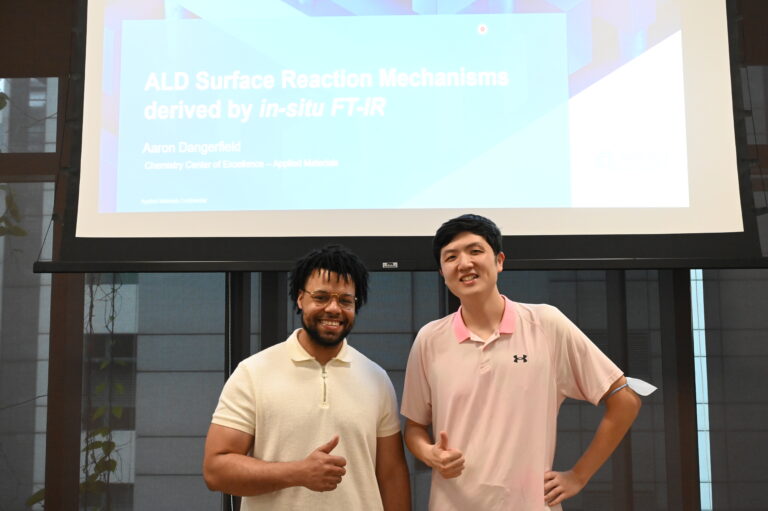
Date and Time: Thursday, 25th January 2024, 3.00pm – 4.00pm
Venue: Blk E7, #03-07, Seminar Room 2
Speaker: Originally from Lafayette, Louisiana, Dr Aaron Dangerfield is a process engineer where his expertise is in Surface Science, particularly XPS and Infrared spectroscopy. He has a Ph.D. in Materials Science and Engineering from UT Dallas under Dr. Yves Chabal.
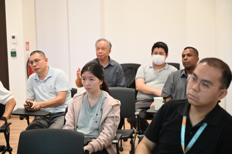
Abstract: ALD Surface Reaction Mechanisms derived by in-situ FT-IR
In this talk, Dr. Aaron Dangerfield will give an overview of the Surface Science capabilities and share some examples of how we apply this tool to understand Atomic Layer Deposition (ALD) reaction mechanisms. Fourier-Transform Infrared Spectroscopy (FT-IR) is widely known as a technique for identifying functional groups in “bulk” compounds through the detection of molecular vibrations. However, under the right conditions, it can be a powerful tool for probing surface structure and precursor adsorption as well. Understanding these mechanisms can give valuable insight into the “how” and “why” some precursor/reactant combinations work, and others do not.
Date and Time: Tuesday, 26 September 2023, 11.00am to 12.00pm
Venue: Block EA, Level 1, Lecture Theatre 7A @ NUS
Speaker: Dr. Satheesh Kuppurao is responsible for Business management of all SPG semiconductor products for Applied Materials, developing and executing new business models, driving business process and productivity improvements, managing growth through investments, and developing external partnerships. He has over 25 years of experience in the semiconductor equipment industry driving product innovation and commercializing technologies. and holds a Ph.D. in Materials Science from the University of Minnesota, Minneapolis.
Abstract: The world today has become more comfortable and fulfilling due to advancements in semiconductor technology. Various processes, such as epitaxy, PVD, CVD, and ALD, create materials, while others like planarization and etching shape them. Processes such as implantation and annealing modify material properties, and CD-SEM and inspection analyze the features. Applied Materials is the largest provider of manufacturing equipment for the semiconductor industry. As manufacturing challenges continue to increase, engineers and technologists are co-optimizing and connecting multiple technologies, enhancing them with sensor data and machine learning to accelerate the development of new solutions. This talk will focus on the critical challenges in semiconductor manufacturing, how innovative technologies developed by Applied Materials are addressing them, and the need for broader collaboration across the industry, academia and government.

Date: Friday, 18 August 2023
Time: 12.00pm to 1.00pm
Speaker: Christian Nijhuis received his Ph.D. degree from University of Twente in 2006 (Cum Laude; top 5%) under the supervision of Profs Jurriaan Huskens and David Reinhoudt. In the group of Professor George M. Whitesides at Harvard University, as a postdoctoral research fellow, he developed a platform formeasurements of charge transport across layers that are one molecule thick. In 2010, he got the NRF research fellowship (3 million dollar). He joined the Department of Chemistry at the National University of Singapore. In 2012, he received the NRF CRP grant to start a new program to develop plasmonic-electronic devices which entered phaseII in 2017 (total funding of 14 million dollar). In 2020, he moved back to the University of Twente as Full Professor to start a new group Hybrid Materialsfor Opto-Electronics. He co-authored >160 peer reviewed papers, received several awards (including Dean’s Chair (2018) and NUS University Young Researcher Award (2016)) and NWO Vici grant (2022)
Abstract: Inspired by the energy efficiency of brains and the ever-increasing demand for miniaturised electronics, there is a drive to develop devices that mimic the dynamic character of neurons and synapses.To achieve this goal, brain-like computing is emulated with energy inefficient and complex silicon-based circuits or with mesoscale memristors, but these approaches still require large amounts of energy.
Date: Monday, 3 April 2023
Time: 11.00am to 12.00pm
Venue: Seminar Room 1 MD1-08-01E Tahir Foundation Building Level 8 Unit 1 E, 12 Science Drive 2, S(117549)
Speaker: Professor F. Ekkehardt Hahn has held prestigious positions at the Free University Berlin and the University of Münster. Besides serving as a Visiting Professor at the National University of Singapore, UC Berkeley, and other esteemed institutions, Professor Hahn is also a member of the European Academy of Science and the Feodor Lynen-Fellowships selection committee.
Abstract: The presentation delves into the synthesis of heterobimetallic NHC complexes using selective metalation methods. Professor Hahn focuses on the reactivity of unsymmetric azolium-azole NHC precursors derived from caffeine. The C2-H azolium site undergoes deprotonation/metalation, resulting in the formation of a mononuclear NHC complex. The C2-iodoazole group, on the other hand, can be metallated through oxidative addition to low-valent transition metals, leading to the formation of heterobimetallic NHC/azolato complexes.
Date: Friday, 10 February 2023
Time: 11.00am to 12.00pm
Venue: Virtual
Speaker: Professor Xianwen Mao, an Assistant Professor of Materials Science and Engineering at the National University of Singapore (NUS), completed his PhD in Chemical Engineering at the Massachusetts Institute of Technology (MIT). His Postdoctoral Research at Cornell University was centered around developing single-molecule/particle techniques for operando functional imaging of complex energy materials. With several patents filed, his research and technological innovations has garnered attention from The New York Times and Chemical & Engineering News.
Abstract: This talk explores the significant role of electrochemical interfaces in addressing climate change, renewable energy, and clean water. The impact of nanostructuring in molecularly engineered soft materials on their electrochemical performance is emphasized, particularly self-assembled nanostructures at electrified interfaces. The presentation also covers the development of state-of-the-art operando functional imaging tools, facilitating a detailed exploration of materials chemistry and properties at the single-entity level. Specifically, (photo)electrochemical catalytic properties of emerging materials relevant to energy and environmental applications are investigated. By uncovering insights at the single-entity level, a more profound understanding of electrochemical interfaces is achieved.
Date: Thursday, 22 July 2022
Time: 3.00 to 4.00pm
Venue: Seminar Room: Eureka 1&2 | 5 Engineering Drive 1, Block E6, Level 6, S(117411)
Speaker: Dr Greg Johnson, Senior Applications Development Engineer from ZEISS Research Microscopy Solution, has more than 25 years in device characterization and failure analysis of electronics. At IBM’s Semiconductor Research and Development Center, he was either the lead or sole failure analysis engineer for defect localization across seven bulk technology node qualifications.
Abstract: Probing methods promise to provide means for characterization of electronic materials and contribute to device tailoring and defect localization in yield management. This talk will provide updates from recent experiments for both the techniques of Conductive Atomic Force Microscopy, and Electron Beam Induced Current in nanoprobing. Results from 5 and 7 nm SRAMs will be discussed and time will be allotted for discussion of new applications.
Date: Saturday, 9 April 2022
Time: 3.00 to 4.00pm
Venue: Seminar Room Eureka 1&2 | 5 Engineering Drive 1, Block E6, Level 6, S117411

Speaker: Professor Lain-Jong (Lance) Li, Chair Professor of the Department of Mechanical Engineering at The University of Hong Kong.
Abstract: With the dimension scaling for future electronics technology nodes, the gate controllability becomes weaker owing to the pronounced source-drain tunneling. Hence, the transistor body thickness needs to be reduced to ensure efficient electrostatic control. New materials with perfect surfaces are therefore needed and 2D semiconducting materials such as TMD monolayers offer a chance to continue the scaling. Meanwhile, these 2D monolayers are sensitive to the scattering from adjacent 3D dielectrics. Thus, a perfect interfacial dielectric layer hexagonal Boron Nitride (h-BN) is needed to suppress the scattering. The growth of hBN and 2D TMD has therefore become a central research topic in modern electronics.
Date: Friday, 8 October 2021
Time: 12.00pm to 1.00pm
Venue: Virtual
Speaker: Dr Chung Jing-Yang, completed his PhD study under the Singapore-MIT Alliance for Research and Technology (SMART) program. Supervised by Professor Michel Bosman and Professor Silvija Gradecak, his Doctoral Research focused on the utilisation of advanced electron microscopy for investigating atomic-scale phenomena in new nanostructured III-nitride optoelectronics. With a specialisation in electron microscopy and expertise in nanotechnology, his work at SMART also involved contributing to the development of commercially viable integrated III-V CMOS chips through nanoscopic elemental failure analysis.
Abstract: With the advent of 5th order abberation correctors in scanning transmission electron microscopes (STEMs), direct imaging of atom positions becomes possible. This allows the unambiguous interpretation of atomic-scale features governing the performances of functional materials, such as optoelectronic devices. In this seminar, a showcase of STEM methods being applied to In-Rich InGaN light-emiting diodes (LEDs) will be presented. Through the use of complementary techniques involving low/high-angle dark-field imaging, electron energy loss spectroscopy (EELS) and cathodoluminescence (CL), direct correlation between crystal defects, crystal strain, phase separation and light emission were obtained.
Date: Friday, 17 September 2021
Time: 12.00pm to 1.00pm
Venue: Virtual
Speaker: Dr. Nur Fadilah Jamaludin was conferred her PhD in 2020 under the Sustainable Earth Programme, offered by the Interdisciplinary Graduate School in Nanyang Technological University (NTU). She majored in Materials Science and Engineering, with her primary research interest geared towards green energy and sustainability. Currently a Research Fellow at ERI@N, she has more than 7 years of research experience on halide perovskite semiconductor materials for various optoelectronic applications including photovoltaics, light-emitting diodes, memory and neuromorphic devices.
Abstract: Unlike antecedent lighting technologies, perovskite based LEDs (PeLEDs) have taken on an almost exponential efficiency trajectory, with state-of-the-art PeLEDs having EQEs exceeding 20% in less than a decade of research. Driven by unique optoelectronic properties such as high colour purity, low defect density and bandgap tunability, perovskites have emerged as a promising contender in the field of light emission. Here in this talk, we’ll walk through what it is that brings about the excitement surrounding perovskites, the evolution of research in this field and what the future holds for perovskites beyond LEDs.
Date: Friday, 26th February 2021
Time: 9.00am to 10.00am
Venue: Virtual
Speaker: Dr Soumyadeep Sinha, obtained a PhD Degree from Indian Institute of Technology (IIT) Bombay, India. He worked as a Postdoctoral researcher in Chonnam National University, Republic of Korea till 2019. He served as an Assistant Professor in the Department of Physics at Madanapalle Institute of Technology adn Science, India until December 2020.
Abstract: Atomic Layer Deposition (ALD) has emerged as a promising and efficient tool for various energy applications due to its unique advantages. In this context, our team has developed custom-built thermal ALD reactors with in-situ facilities. Our research focuses on ALD of wide bandgap binary compounds, specifically zinc-based materials such as oxides, nitrides, and sulfides. Additionally, we explore the possibilities of doping these materials to create transparent conducting materials for electronic and optoelectronic applications.
Date: Friday, 19th February 2021
Time: 10.00am to 11.00am
Venue: Virtual
Speaker: Dr Muhammed Juvaid received his Doctoral Degree in Physics from Madras and National University of Singapore (IITM-NUS Joint PHD Programme) and is currently working as a Research Fellow at AMAT-NUS Corporate Lab. He completed his Masters Degree (M Tech) from IIT Madras, India. He has worked as a visiting Research Fellow at Bristol Center of Functional Nanomaterials, University of Bristol, UK. His research interests include growth and device fabrications of various two-dimensional materials.
Abstract: Our focus is on obtaining graphene and related materials through laser-assisted growth, particularly utilizing large-area films grown by pulsed laser deposition. Graphene Oxide (GO) and reduced Graphene Oxide (rGO) are commonly used as precursors for graphene. To achieve scalable and reproducible growth of uniform rGO thin films, we have explored the pulsed laser deposition (PLD) technique at lower process temperatures. These rGO films exhibit superior properties compared to chemically synthesized rGO, including precise thickness control, smooth surfaces, and potential for heterostructures. We have demonstrated wafer-scale growth of rGO films by PLD, showcasing their potential applications as p-type transparent conducting thin films in various optical and electrical fields.
Date: Friday, 5th February 2021
Time: 11.00am to 12.15pm
Venue: Virtual
Seminar Topics
Speakers: PhD Graduate Students under the AMAT-NUS Corporate Laboratory.
1. “Charge Carrier Mobility and Series Resistance Extraction in Two-Dimensional Field-Effect Transistors: Towards an Universal Technique” by Mr Chien Yu-Chieh
An universal extraction that can separately determine the intrinsic mobility and source-drain series resistance in two-dimensional field-effect transitors is explored. The merit of the present method is reinforced by demonstrating the applicability to various 2D channel materials with top and bottom gate configurations.
2. “Memory Device based on HfO2 Doped Ferroelectric Material and its Application in Neuromorphic” by Mr Zhou Zuopu
Focusing on the ferroelectric non-volatile memory devices, we developed a ferroelectric thin film with a low thermal budget and further integrated it with the semiconductor and proposed a novel metal-insulator semiconductor capacitive memory device. We are also exploring the application of the emerging non-volatile memory devices in the neuromorphic computing technology and trying to demonstrate the concept by the co-design of the material, device and circuit.
3. “Ferroelectric Materials based Memories and Transitors for AI Hardware Applications” by Mr Tsai Shih-Hao
Ferroelectric field effect transistor based in-memory computing is a promising methodology for increasing the efficiency of deep neural network. However, the polarization, breakdown strength and analog performance of FeFET remain to be improved with the aim of demonstrating multiple analog memory states and high pattern recognition accuracy. This work paves a path for further improvement in neuromorphic computing,
Date: Friday, 11th December, 2020
Time: 2.00pm to 3.00pm
Venue: Virtual
Speaker: Dr Tan Sze Chieh have recently completed her PhD study under the NUS Graduate School for Integrative Sciences and Engineering. Her research area was in Analytical Chemistry, with focus on the development of sample preparation methods for the extraction and analysis of chemical compounds in environmental water samples. During her undergraduate studies (Materials Chemistry) at NUS, she also has an opportunity to work on the research and development of polymeric-based composites for biomedical applications.
Abstract: In this study, we focused on the design and development of novel extraction materials, including graphitic carbon nitride and a metal-organic framework and its derivative. We also explored the integration of different solvent and absorption-based extraction techniques to automate the sample preparation process. These newly developed methods were optimized, validated, and evaluated by enriching and analyzing contaminants in genuine environmental water samples. As the field of green chemistry gains prominence in analytical chemistry, our research contributes to the advancement of efficient and sustainable sample preparation for trace analyte analysis.
Date: Friday, 2nd October 2020
Time: 11.00am to 12.15pm
Venue: Virtual
Seminar Topics
Speakers: PhD Graduate Students under the AMAT-NUS Corporate Laboratory.
1. “Exploring new strategies for preparation of macrocycles, COFs and belts” by Mr Zhu Jun
Friedlander Synthesis, in general, can be defined as an acid-or based-catalyzed condensation followed by a cyclodehydration to form quinoline structure. As an efficient reaction, it has been extensively explored since 1882. Now, we wish to explore the possibilities to prepare Macrocycles, Covalent Organic Frameworks (COFs) and Belts based on Friedlander synthesis.
2. “A low-voltage diffusive memristor using 2D SnS” by Ms Lu Xiu Fang
Memristive devices are promising candidates to emulate neuromorphic computing. Here, a diffusive memristor is fabricated by using 2D SnS, which possesses a very low switching voltage. Moreover, in this memristor, both short-term and long-term plasticity of biological synapses can be emulated, opening a possibility in neuromorphic computing.
3. “2D Supramolecular Self-Assembly Monolayers via Halogen Bonds” by Ms Wang Lu Lu
Self-assembly monolayers (SAMs) have become a good choice to be used for “bottom-up” approach, thousands of research groups are working on how to make conformed good quality SAMs and the corresponding applications. At the same time, as the development of computational chemistry, we wish to use it to understand more detailed mechanisms.
Date: 15th September 2020
Applied Materials South East Asia hosted an online panel entitled “Innovate anywhere; collaborate everywhere”. The event has been organised by the AMAT-NUS co-director Dr John Sudijono and one of the panelist was Prof. Silvija Gradecak-Garaj, who is the other co-director of our lab.
Effective Suppression Of Current Collapse In Both E- and D-mode AIGaN/GaN HEMTs on Si by [NH4)2Sx] Passivation
Date: Friday, 22nd May 2020
Time: 12.00pm to 1.00pm
Venue: Virtual
Speaker: Vicknesh Sahmuganathan is a researcher with expertise in optoelectronic devices. He completed his Master of Science degree at Nayang Technological University while working at the Institute of Materials Research and Engineering. During his time at Temasek Laboratories, he focused on developing Gallium Nitride-based high mobility electron transistors and monolithic microwave integrated circuits for various applications. Currently, he is employed at Applied Materials Singapore Technology where he contributes his knowledge to the AMAT-NUS Corporate Lab.
Abstract: An effective suppression of drain current collapse was realised in both Enhancement mode and Depletion (D) mode AIGaN/GaN High electron mobility transitors (HEMTs) on 4-inchSilicon (111) by Ammonium Sulfide passivation. The current collapse was studied using the pulsed current-voltage characteristics with the pulse width of 200ns and pulse period of 1ms. With reference to the AIGaN/GaN HEMTS without sulphur passivation, about 30% of the drain current collapse was suppressed for drain quiescent biases of 25 to 30V. Obtaining low current collapse is essential to demonstrate high power GaN HEMTs.
Date: Monday, 27 March 2020
Time: 11.30am to 12.30pm
Venue: Virtual
Speaker: Dr Salim El Kazzi joined IMEC as a research scientist. Dr. El Kazzi’s work includes pioneering the first plasma-source MBE of TMDC-MX2 materials and leading the lab and fab of 2D MX2-based materials.Currently, he serves as a Senior Research Fellow at NUS-Applied Materials Corporate Lab, where he explores deposition and etching techniques for both FEOL and BEOL applications.
Abstract: The discovery of Graphene and its related 2D materials has sparked a wave of research and innovation across various fields. These materials hold promise for applications in water treatment, clean energy, sensing, optics, and the convergence of 5G communications with the Internet of Things (IoT). However, the lack of high-quality synthetic materials and production-friendly machines has hindered their mass production. In this talk, the focus is on the deposition and epitaxy of (Mo,W)(S,Se)2 semiconductors on commercial substrates, enabling the integration of controlled 2D layers on large areas. Challenges related to materials integration and growth conditions are discussed, along with the growth of MX2 on 300 mm Si wafers. The talk concludes with a strategy for integrating 2D materials into a fabrication production environment, offering insights for future CMOS technology.
Date: Friday, 7 February 2020
Time: 11.30am to 12.30pm
Venue: E6-06-02/03 Eureka 1&2
Speaker: Dr Paul Mehlmann, AMAT-NUS Corporate Lab Research Fellow
Abstract: To enhance the donor strength of phosphines, a new approach to highly electron-rich phosphines based on the use of imidazolin-2-ylidenamino groups directly attached to the phosphorus atom is reported. The unique electronic properties of these phosphine and phosphorandiylium provide new prospects in transition metal catalysis and in small molecule activation.
Date: Tuesday, 28 January 2020
Time: 12.00pm to 1.00pm
Venue: Seminar Room 2 (MD1-08-03E)
Speaker: Professor Jung Yousung, Department of Chemical and Biomolecular Engineering, KAIST, South Korea
Abstract: Discovery of a new material with desired properties is the ultimate goal of materials research. A promising way to significantly accelerate the latter process is to incorporate all available knowledge and data to plan the synthesis of the next material. In this tallk, a few initial frameworks developed along the line to perform machine-learned density functional calculations to predict the properties of a material catalyst using simple representations as well as to inverse design new materials with a target property using materials deep generative model.
Date: 12 to 13 December 2019
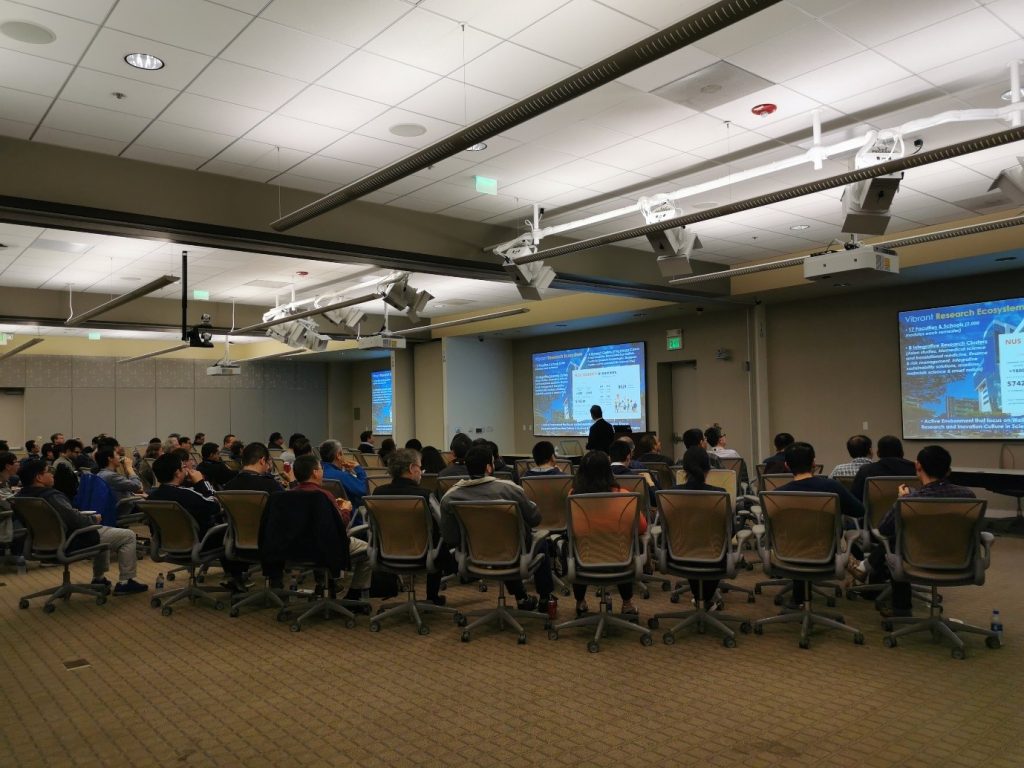
Applied Materials-NUS Corporate Lab Co-Directors led a team of NUS researchers and staff for a two full day visit to Applied Materials @ Santa Clara, USA.
Read more by clicking here.
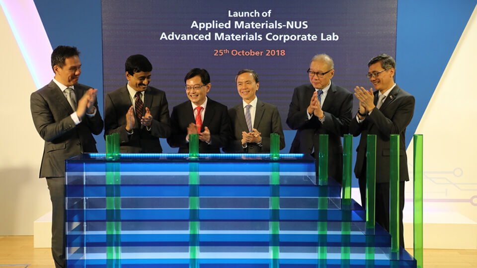
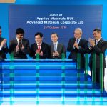
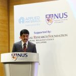
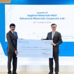
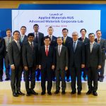
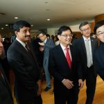
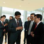
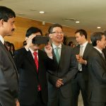
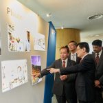
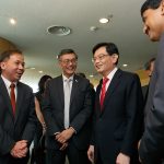
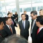
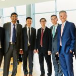
Applied Materials-NUS Advanced Materials Corporate Lab was officially launched by Guest-of-Honour Finance Minister and Chairman of NRF Mr Heng Swee Keat, NUS President Professor Tan Eng Chye and Applied Materials Senior Vice President Dr Prabhu Raja.
Click to read more about the NUS research news on the $70m next generation semiconductor advanced materials corporate lab.